Ƶ�ʺ�����ʱ��Դ�������ſؽ��䵪���ѳ������ʺ���ò��Ӱ��
��Դ�ڿ����й���ɫ����ѧ��(Ӣ�İ�)2019���12��
�������ߣ�Saeed GHASEMI Ali Reza FARHADIZADEH Hamid GHOMI
����ҳ�룺2577 - 2590
�ؼ��ʣ���������ſؽ���(HiPIMS)�������ѣ���Ӧ�淨(RSM)���������ʣ��������
Key words��high powder impulse magnetron sputtering (HiPIMS); titanium nitride; response surface methodology (RSM); deposition rate; analyses of variance (ANOVA)
ժ Ҫ�����ô�������ſؽ���(HiPIMS)���ڲ�ͬƵ��(162~637 Hz)������ʱ��(60~322 ��s)�����£��������ѱ�Ĥ�����ڹ�����ϡ�������Ӧ�淨�о�Ƶ�ʺ�����ʱ��Ե������Ρ�����ȡ������֯��ЭͬӰ�죬�ر��ǶԺ㶨ʱ�䡢ƽ������Ϊ250 W�����µ����ѳ������ʵ�Ӱ�졣�ֱ���XRD��FESEM�Գ�����Ĥ�ľ���ṹ����ò���з����������������Ʒ�ij�������������ʱ�������Ƶ���кܴ�Ĺ�ϵ������������4.5~14.5 nm/min֮��仯���ع鷽�̺ͷ��������ʾ����Ƶ��Ϊ537 Hz������ʱ��Ϊ212 ��sʱ�������������Ϊ(17��0.8) nm/min��ʵ��������ô������µij�������Ϊ16.7 nm/min����Ԥ��ֵ�ǺϽϺá�
Abstract: Titanium nitride thin films were deposited on silicon by high power impulse magnetron sputtering (HiPIMS) method at different frequencies (162-637 Hz) and pulse-on time (60-322 ��s). Response surface methodology (RSM) was employed to study the simultaneous effect of frequency and pulse-on time on the current waveforms and the crystallographic orientation, microstructure, and in particular, the deposition rate of titanium nitride at constant time and average power equal to 250 W. The crystallographic structure and morphology of deposited films were analyzed using XRD and FESEM, respectively. It is found that the deposition rate of HiPIMS samples is tremendously dependent on pulse-on time and frequency of pulses where the deposition rate changes from 4.5 to 14.5 nm/min. The regression equations and analyses of variance (ANOVA) reveal that the maximum deposition rate (equal to (17��0.8) nm/min) occurs when the frequency is 537 Hz and pulse-on time is 212 ��s. The experimental measurement of the deposition rate under this condition gives rise to the deposition rate of 16.7 nm/min that is in good agreement with the predicted value.
Trans. Nonferrous Met. Soc. China 29(2019) 2577-2590
Saeed GHASEMI, Ali Reza FARHADIZADEH, Hamid GHOMI
Laser and Plasma Research Institute, Shahid Beheshti University, Evin 1983963113, Tehran, Iran
Received 2 March 2019; accepted 28 August 2019
Abstract: Titanium nitride thin films were deposited on silicon by high power impulse magnetron sputtering (HiPIMS) method at different frequencies (162-637 Hz) and pulse-on time (60-322 ��s). Response surface methodology (RSM) was employed to study the simultaneous effect of frequency and pulse-on time on the current waveforms and the crystallographic orientation, microstructure, and in particular, the deposition rate of titanium nitride at constant time and average power equal to 250 W. The crystallographic structure and morphology of deposited films were analyzed using XRD and FESEM, respectively. It is found that the deposition rate of HiPIMS samples is tremendously dependent on pulse-on time and frequency of pulses where the deposition rate changes from 4.5 to 14.5 nm/min. The regression equations and analyses of variance (ANOVA) reveal that the maximum deposition rate (equal to (17��0.8) nm/min) occurs when the frequency is 537 Hz and pulse-on time is 212 ��s. The experimental measurement of the deposition rate under this condition gives rise to the deposition rate of 16.7 nm/min that is in good agreement with the predicted value.
Key words: high powder impulse magnetron sputtering (HiPIMS); titanium nitride; response surface methodology (RSM); deposition rate; analyses of variance (ANOVA)
1 Introduction
Transition metal nitrides such as CrN, TiN, and AlN have a wide range of industrial applications because of their high hardness, corrosion and wear resistance, and thermal stability properties [1-8]. The studies have demonstrated that the properties of TiN thin films are strongly dependent to the deposition parameters, e.g., the substrate temperature, the nitrogen partial pressure, the ion energy, and the incident ion-to-metal flux ratio [9-12]. Magnetron sputtering (MS) is of huge interest due to the relatively high deposition rate, the high quality of films, the low contamination in the process, and the capability to control the microstructure and properties of the deposited layers. However, since the ionization rate in the plasma of MS is not sufficiently high, it is quite difficult to reach a very dense layer with favorable crystallographic orientation. For instance, MS normally leads to (111) preferred crystallographic orientation, while (200) orientation yields to higher elastic moduli [13,14], which is of more interest if the enhancement of mechanical properties is aimed.
On the other hand, the high power impulse magnetron sputtering (HiPIMS) technique is such a method to provide a high ionization rate as well as a high degree of cleanliness in the coatings [15-19]. The high peak power in HiPIMS discharge increases the density of the plasma and the ionization degree of sputtered materials, leading to high-quality thin films, fully dense structure, low surface roughness, superior hardness, low friction coefficient, corrosion and wear resistance properties, and droplet free coatings [20,21].
The ion-to-neutral flux ratio in the HiPIMS deposition system is related to the pulse-on time duration and operation modes (single- or multi-pulse); correspondingly, the microstructure and morphology of coatings could be modified. When ultra-short pulses and multi-pulses of HiPIMS are used, the ratio of ions with low and intermediate energy increases, which is of interest [11]. It is also reported that the increment of Ti+ flux as well as the total ion flux modifies the microstructure from columnar to fully dense, and enhances the hardness, the elastic modulus, and the adhesion to the substrate [11]. Besides, it is shown that the modulation of the pulse frequency results in a higher degree of ionization, and consequently, the better control of texture could be obtained [22]. However, since the deposition rate of the HiPIMS system is less than that of the conventional DC magnetron sputtering (DCMS), many studies have been carried out to improve the deposition rate. For instance, GANESAN et al [23] addressed the influence of an external magnetic field by inserting a solenoid coil between the target and substrate on the peak current, the ion current, and the deposition rate.
The current discharge waveforms of HiPIMS, which are of utmost importance in determining the characteristic of plasma and deposited layers, are thoroughly reviewed in the literature [23,24]. GUDMUNDSSON et al [25] divided the HiPIMS current discharge waveforms into five different phases: the ignition phase, the current rise phase, the gas depletion, the plateau/runaway region, and the afterglow phases. They claim that the plateau/runaway region could suitably be explained and categorized by degree of self-sputtering (��ss). When ��ss<0.1, the discharge is DCMS-like, when 0.1<��ss<1, the partial self-sputtering takes place and when ��ss>1, the self-sputtering is great and runaway section rather than plateau section is observed. Furthermore, the production and disappearance of ions and secondary electrons are primary parameters to analyze the current discharge waveforms [26,27]. In addition, the target material and the discharge voltage alter the current discharge waveform of HiPIMS [28,29].
Although numerous studies have considered the effect of HiPIMS parameters on the properties of thin films [30-34], to our knowledge, no literature discussed the simultaneous influence of frequency and pulse-on time of a HiPIMS system on the properties of thin films from a statistical viewpoint. Response surface methodology (RSM), which was presented in 1951 [35], uses statistical techniques to investigate the influence of independent variables on given properties. This method not only decreases the number of experiments but also provides a deep understanding of the interrelation of processing parameters. Furthermore, ANOVA is widely employed to assess the influence of each parameter on the specific properties which is also used in some literatures [36,37] to investigate the physical vapor deposition process.
The current work aims to investigate the simultaneous effect of frequency and pulse-on time on the microstructure, texture coefficient, morphology, and deposition rate of titanium nitride. Therefore, a statistical approach, RSM, is performed to design the experiments and then ANOVA and regression model are used to analyze the obtained results. Since a deep understanding of the results is our goal, in the beginning, the feature of our lab-made HiPIMS is thoroughly discussed. It also helps validate the performance of our system as it is compared to the literature.
2 Experimental
2.1 Response surface methodology (RSM)
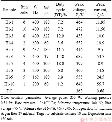
In this work, RSM with central composite design (CCD) was employed to explore the effect of the pulse-on time and the frequency on the properties of TiN layers (Fig. 1). Based on trial and errors, the upper and lower bounds of variables were established (Table 1) and ��, the distance of each axial point in CCD from the center, was set to be 1.19 in which the ranges of frequency and pulse-on time do not exceed the capability of the HiPIMS system. In this method, it is possible to determine the linear, quadratic, and interaction effects of frequency and pulse-on time on the deposition rate of TiN layers. The experiments were designed using Minitab (Version 17) software in 10 runs shown in Table 2. The experiments were arranged randomly so that the possible biases in responses, originating from target erosion, cleanliness of the system, etc., would be minimized. The samples Hi-1 and Hi-2 are replicate in order to decrease the pure error of the experiments.
2.2 Film preparation
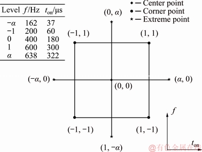
Fig. 1 Schematic of CCD performed to deposit TiN layers where f and ton stand for frequency and pulse-on time, respectively
Table 1 Values of deposition process variables

Table 2 Deposition parameters for HiPIMS and DCMS
All of the experiments have been carried out by a lab-made vacuum deposition system that is explained elsewhere [13]. Titanium nitride layers were deposited by DCMS and HiPIMS. The HiPIMS system is designed and manufactured in our laboratory. The power supply of HiPIMS can provide pulses with pulse-on time and frequency in the range of 20-500 ��s and 100-1500 Hz, respectively. The HiPIMS power was supported by a DC power supply (1-1000 V and 1 A). In this system, the maximum target voltage and current could rise up to 1000 V and 100 A, respectively.
The specimens used in this work were Si (100) cut into 1 cm �� 1 cm. The samples were ultrasonically cleaned with pure acetone and ethanol. Then, the substrate surfaces were argon ion bombarded for 20 min as a final step for surface preparation. Ar ion bombardment of the substrate is normally carried out in order to remove contamination and oxide layers from the substrate surface. The purity of the titanium target, argon and nitrogen gas used in the deposition process were 99.7%, 99.995% and 99.995%, respectively. The dimensions of the target were 5 and 0.6 cm in diameter and thickness, respectively.
For each experiment of HiPIMS, the voltage was regulated to reach the constant average power equal to 250 W. The deposition parameters including duty cycle, peak voltage, peak current, deposition pressure, gas flow ratio, substrate temperature, bias voltage, etc are given in Table 2.
2.3 Discharge and film characterization
Discharge voltage and current were measured by Tektronix TDS 2024B digital oscilloscope equipped with a high voltage probe and a current probe (0.3 �� shunt resistor). The average power is calculated as follows:
 (1)
(1)
where Pa is average power; T, Ud(t), and Id(t) are pulse period, discharge voltage and discharge current, respectively. The presence of Ar and Ti atoms and ions in plasma was detected by Emerald spectrometer (C0R10, TEKSAN Co.) with spectral resolution equal to 0.5 nm. The structure, crystallite size, and texture coefficient of coatings were measured by Philips X-ray diffractometer with the wavelength of Cu K�� equal to 1.54056  . FESEM was also used to measure the film thickness and to study the film microstructure and surface morphology (MIRA3TESCAN-XMU). The deposition rate was calculated from the measured thickness divided by the deposition time [31,37,38].
3 Result and discussion
3.1 HiPIMS discharge characteristics
Since our HiPIMS system is lab-made, in this section, we aim to shed the lights on the discharge characteristic of the HiPIMS. Because the current waveforms and I-V characteristics of HiPIMS indicate the feature of the system, they are investigated and compared to the literature.
3.1.1 Effect of pulse-on time on current waveforms
The influence of pulse-on time on the evolution of HiPIMS discharge current is studied at 100 and 400 ��s pulse-on time while the frequency and the pressure are equal to 100 Hz and 1.33 Pa, respectively. The discharge peak voltages vary in the range of 310-474 V when the pulse-on time is 400 ��s (Fig. 2(a)) and 427-636 V when the pulse-on time is 100 ��s (Fig. 2(b)). As seen in Fig. 2(a), when the discharge peak voltage is higher than 384 V, the current waveforms consist of an initial peak (around 60 ��s) followed by a plateau current level. In other words, a sharp increment of the current occurs which is related to the high ionization rate of argon in the very beginning of the process. Afterwards, owing to the rarefaction phenomenon [39], the current decreases with a moderate slope into a constant value. For those of peak voltages less than 384 V, the current increases to a specific value and it almost remains constant. For a shorter pulse-on time of 100 ��s (Fig. 2(b)), the current continuously and gently rises when the peak voltage is lower than 449 V. However, for higher peak voltage, the current sharply increases to a maximum value and then, it quite gently decays and unlike the current waveforms for the pulse-on time of 400 ��s, they possess neither the plateau segment nor noticeable peak. It is worth mentioning that the upper limit of the discharge voltage is directly attributed to the features of the deposition system including magnetic field configuration, gas compositions, and the DC power supply; this is why no higher discharge voltage is tested here.
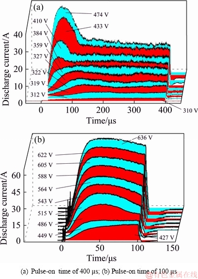
Fig. 2 Current pulse shapes at different constant voltages for titanium target in argon at 1.33 Pa and 100 Hz
According to WU et al [24], the current waveforms shown in Fig. 2(a), with voltages more than 384 V, could be classified in mode 5 which contains 5 distinct phases including ignition phase (~10 ��s), current rise phase (10-80 ��s), gas depletion phase (80-130 ��s), plateau phase and afterglow phase described thoroughly in Ref. [25]. In this mode, the sputtering rate of the target material, the emission of secondary electrons as well as the multiply charged metal ions are considered low and therefore, after the current peak where the gas depletion occurs, owing to lack of multiply charged ions, the decrement of discharge current continues until plasma reaches to such an equilibrium which is defined in Ref. [24] as a balance between the production and disappearance of metal ions in the plasma. Under this circumstance, the composition and the density of plasma remain almost constant until the end of the pulse. Note that the value of the plateau current is less than 20 A, indicating the self-sputtering parameter (��ss) is not very high [25]. Because the applied voltage (or equivalently the sheath voltage) provides sufficient energy to create multiply charged metal ions, it seems that the observed low self-sputtering is due to the low applied voltage.
The current waveforms at 100 ��s (Fig. 2(b)) are distinctively different from those at 400 ��s which could be linked to the duration of pulse-on time. According to Ref. [25], Fig. 2(b) is composed of only three phases: ignition phase, current rise phase, and gas depletion phase. As implied by Ref. [28], the pulse-on time around 100 ��s is not long enough to generate the highly charged ions necessary for the plateau or runaway phase. As seen, there is a wide current peak that is about to fade away when the voltage increases. In other words, when the applied voltage increases, the decay of the current after the peak decreases. As the current reaches to the peak, the gas depletion phase starts which causes the current to decrease. However, increasing the voltage promotes the energy of emitted secondary electrons, the production of highly charged metal ions, and partial self-sputtering, leading to less decay of the current after the peak.
ANDERS et al [28] also investigated the current waveforms of the titanium target in constant voltage. They showed that the current waveforms of titanium target in low voltage were the same as mode 5 (Fig. 2(a)), while in the higher voltage, the character of waveforms current differs from our work, which could be attributed to the impedance of the plasma. The higher the impedance of the plasma, the higher the value of discharge voltage is, leading to different current waveforms. If the plasma impedance of our system increases, the higher voltage can be applied, and under this condition, the threshold voltage for high density plasma could be achieved [40], resulting in different waveforms, as seen in Ref. [28].
3.1.2 Effect of pressure on HiPIMS discharge characteristic
The HiPIMS current waveforms at different pressures have also been studied for the titanium target, where the pressure was altered from 0.53 to 3.5 Pa with a frequency of 200 Hz. In order to further understand the influence of pressure on the current waveforms, two series of experiments were carried out at different pulse-on times equal to 100 and 300 ��s with a constant voltage of 460 and 370 V, respectively, as depicted in Fig. 3. As seen, the onset of the discharge current is delayed in low pressure. When the pressure is 0.53 Pa, the higher the pulse-on time (300 ��s), the more the delay time is, which stems from the lower applied voltage in 300 ��s as well as the lower rate of Ar ionization. When the pressure is higher than 0.8 Pa, the delay time almost vanishes because the ionization happens nearby the target. YUSHKOV and ANDERS [41], who studied the current onset theoretically and experimentally, reported that the increment of working pressure gives rise to the higher rate of efficient initial electrons collision with argon atoms, especially, in the vicinity of the target. Therefore, the higher the pressure, the less time the impact of ions onto the target surface is needed, resulting in shorter delay time. Moreover, as seen in Fig. 3(b), the further increase in pressure leads to a higher rate of argon ionization and subsequently, a sharp current peak could be observed [42].
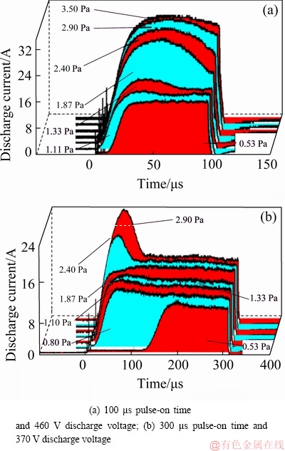
Fig. 3 Current waveform of titanium target at different pressures (200 Hz repetition pulse)
3.1.3 I-V characteristic of DCMS and HiPIMS system
In order to study the plasma impedance, the current-voltage relation is studied here: at first, for the DCMS system and then for HiPIMS system. In the discharge of magnetron sputtering, the relation of the discharge voltage with discharge current is given by the following relation [39,43]:
 (2)
(2)
where Id is the discharge current, Vd is the discharge voltage, k is the geometric coefficient, and the power n is a value that characterizes the magnetron sputtering system, which is generally in the range of 3-15 [44,45], likely to be about 8.5 [39,46].
In DCMS systems, the value of n explains the condition of electron trapping and the number of charge carriers in front of the target [44], as well as the plasma impedance. If n is high, it means that the impedance is low, i.e., much change in discharge current is accompanied by a slight change in the discharge voltage, indicating a weak ionization in the plasma [47]. Figure 4 displays the graph of I-V characteristics in DCMS and HiPIMS system at frequencies equal to 200, 400 and 600 Hz. The measured exponent for the I-V graph of DCMS in Fig. 4 is equal to 10.2 (n=10.2).
The current density-voltage characteristics of HiPIMS discharge at frequencies of 200, 400 and 600 Hz are also shown in Fig. 4. As seen, the impedance of plasma generated through HiPIMS changes with the frequency and the applied voltage that is covered in detail in Ref. [46].
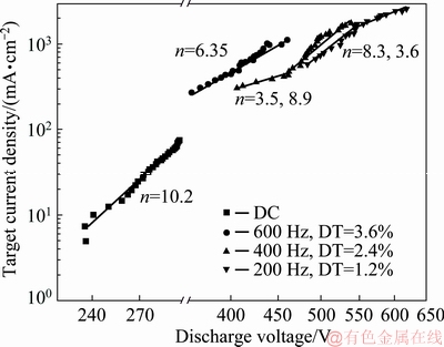
Fig. 4 Current density-voltage characteristics for DCMS and HIPIMS at frequencies of 200, 400 and 600 Hz
3.1.4 Current waveforms of HiPIMS in deposition conditions
As explained in Section 2.1, the experiments were carried out in 10 runs. Since Hi-1 and Hi-2 are the same, there are 9 distinct conditions of deposition. In Fig. 5, the current waveforms of each condition are depicted. For better presentation, the related parameters such as duty cycle, peak power, peak current, and peak voltage are added in each current waveform graph. These current waveforms (Fig. 5) could be divided into three different classes in terms of their general shape regardless of the peak current, the peak power, and the peak voltage.
The typical optical emission spectroscopy (OES) of each class, showing the average amount of Ti+, Ti, Ar+, and Ar during the deposition process, is also presented in Fig. 6. As the used OES is not capable of detecting wavelength below 300 nm, we, unfortunately, could not talk about the presence of multiply charged titanium ions.
The current waveforms of Class I, including Hi-3, Hi-5 and Hi-7, have three phases: ignition, current rise, and gas depletion with no plateau/runaway phase unlike the ones mentioned in Section 3.1.1. Besides, the OES of this class (Fig. 6(c)) shows that the ratio of titanium ions to neutral titanium is around unity, which is more than the ratio in bulk plasma of DCMS (Fig. 6(d)). This indicates that even at large duty cycle (more than 10%), the ratio of metal ions to neutral ones are much higher than that in DCMS.
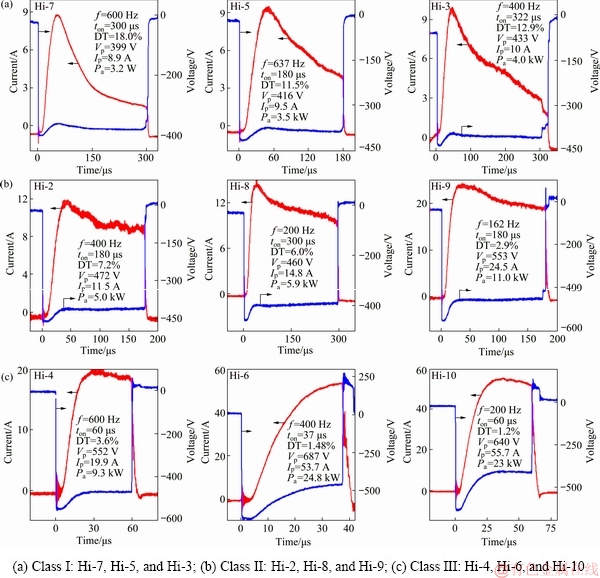
Fig. 5 Current waveforms at deposition conditions divided into three different classes
Although the Class II (Hi-2 (Hi-1), Hi-8, and Hi-9) has more or less the same shape of Class I, the decrease of the current after the initial peak is much less, implying a mechanism to compensate the rarefaction process. These graphs are more similar to Fig. 2(a) with a plateau phase. The OES results of Class II represent the existence of more Ti ions in comparison with the first class (Fig. 6(b)). Since singly charged titanium does not possess enough potential energy to emit secondary electrons [48], the plateau phase in this class is attributed to the presence of multiply charged titanium ions, causing the partial self-sputtering (��ss), which is likely more than the ��ss in Class I.
The Class III, including Hi-4, Hi-6, and Hi-10, has a similar shape to Fig. 2(b), which could be due to the pulse length less than 60 ��s. As stated earlier, when the pulse duration is less than 100 ��s, neither the creation of multiply charged metal ions nor partial sputtering could occur. However, the ratio of Ti+ to Ti is large (Fig. 6(a)), in particular for Hi-6 and Hi-10 with the highest peak power around 24 kW, indicating that the bulk plasma is composed of more metal ions.
3.2 Morphology and microstructure
Since the XRD patterns of each HiPIMS class are very similar, only one typical XRD pattern of each class and DCMS thin film are depicted in Fig. 7. As seen, the films are composed of crystallines with different preferred growth planes including (111), (200) and (220). However, the (200) orientation in all HiPIMS samples, regardless of deposition conditions, is predominant. The preferential growth orientation is directly attributed to the minimization of totally free energy, which is the sum of surface energy, strain energy, and stopping energy [49,50]. Titanium nitride, as shown in Fig. 7, crystallizes in NaCl type FCC structure in which (111) planes have the lowest strain energy because of elastic modules anisotropy [51], and (200) and (220) planes have the lowest surface energy and stopping energy, respectively [52]. According to Fig. 7, in the thin films deposited by DCMS, (111) is preferential growth orientation; while in HiPIMS specimens, (200) plane is preferential.
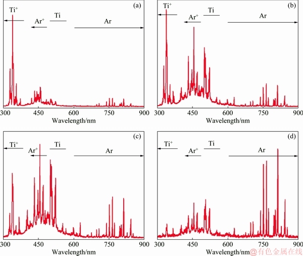
Fig. 6 OES results of HiPIMS ((a) Hi-6 (Class III), (b) Hi-2 (Class II), (c) Hi-7 (Class I)) and DCMS (d)
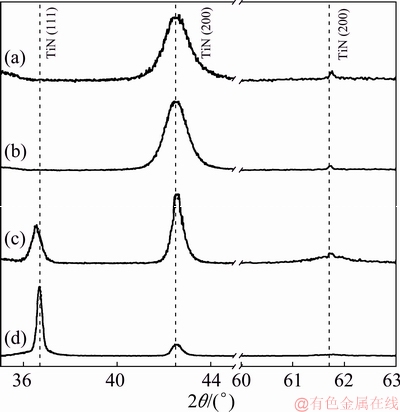
Fig. 7 XRD patterns of HiPIMS ((a) Hi-6 (Class III), (b) Hi-2 (Class II), (c) Hi-7 (Class I)) and DCMS (d)
In PVD systems, the chemical composition of impinging particles onto the substrate defines the texture, the morphology, and the density of layers [53]. When the ratio of metal ions to neutral metal is low, at the beginning of the deposition, the growth orientation is a mixture of (111) and (200) while the preferred orientation varies to (111) by increasing the thickness. In contrast, the high ratio of ion to neutral metals results in the dominance of (200) texture [53].
In reactive HiPIMS deposition systems, with the atmosphere of Ar and N2, the value of N+ ion is higher compared to DCMS systems [54]. Furthermore, in HiPIMS, the ratio of metal ions to neutral metal (Ti+:Ti0) and nitrogen atomic ion to nitrogen molecule ion (N+:N2+) is proportionally associated with the discharge peak current. HiPIMS discharge produces a reasonable amount of nitrogen atomic ion and metal ion with a relatively large ratio of N+:N2+ and Ti+:Ti0 [55]. In HiPIMS discharge, if the discharge peak current is high, the ratios of N+:N2+ and Ti+:Ti0 increase, which leads to preferred growth orientation of (200). On the other hand, if the discharge current is low, the ratios of N+:N2+ and Ti+:Ti0 are low, leading to a strong (111) orientation growth. In addition, the density of thin films decreases when these ratios in discharge reduce [55].
Similarly, the preferred orientation of (111) in the DCMS sample is due to the low ratio of metal ions to neutral metals as well as the high thickness of the layer. In the layers deposited by HiPIMS, Class I, with the lowest discharge current (Fig. 5), the weak (111) growth orientation appears. Indeed, increasing the discharge current leads to the increase of the ratios of N+:N2+ and Ti+:Ti0 in which the ion bombardment onto the substrate surface rises and the suppression of (111) growth orientation occurs.
The crystallite size, texture coefficient, and thickness of HiPIMS and DCMS samples are listed in Table 3. The crystallite size of (111) and (200) of DCMS are 59.8 and 36.1 nm, respectively. The value of crystallite size of (111) and (200) for the layers deposited by HiPIMS is lower than those deposited by DCMS. Three samples of HiPIMS with (111) peak, Class I, have similar current waveforms (Fig. 5). Therefore, the (111) growth could be correlated with the descending part of the current waveforms in Fig. 5. When the current is low, the behavior could be very similar to DCMS in which (111) growth orientation is ordinarily dominant. Because the crystallite size and texture coefficient of HiPIMS samples do not change notably, the statistical approach to analyze the effect of pulse-on time and frequency is not feasible.
Table 3 Crystallite size, texture coefficient, and thickness of layers deposited by DCMS and HiPIMS
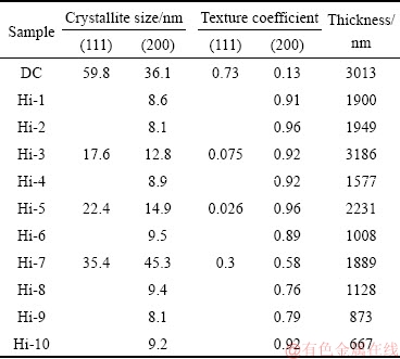
Figure 8 shows the FESEM cross-section images of titanium nitride layers. FESEM images of the layers deposited by HiPIMS are arranged according to their classes. In the layer deposited by DCMS, the film has an intercolumnar spacing, reducing the mechanical properties of the layers [56]. The low ratio of gas ion to the neutral metal gives rise to dome structure [55,57,58] of surface as well as preferred (111) orientation. In titanium nitride thin films, the preferred growth orientation of (111) plane and the dome morphology promote voided intercolumnar structure, which is the result of a shadowing effect [59,60]. The increase in the discharge current leads to the rise of adatoms mobility on the surface substrate, resulting in a preferred (200) orientation growth, a loss of intercolumnar boundaries and the obtention of a denser structure [55]. Moreover, for the sake of comparison, the top-view FESEM images of titanium nitride layers deposited by DCMS and HiPIMS system (sample Hi-7) are shown in Fig. 9. In Fig. 9(a), the layer has pyramid-like surface and pinhole defects (pointed out by white circles) are observed; while in Fig. 9(b), the layer is pinhole-free with a wrinkled surface (pointed out by dark circles). It is obvious that Hi-7 layer has a denser structure compared to DCMS layer even though the cross-section of Hi-7 implies that it does not possess the densest structure among the HiPIMS specimens.
3.3 Statistical analyses of deposition rate
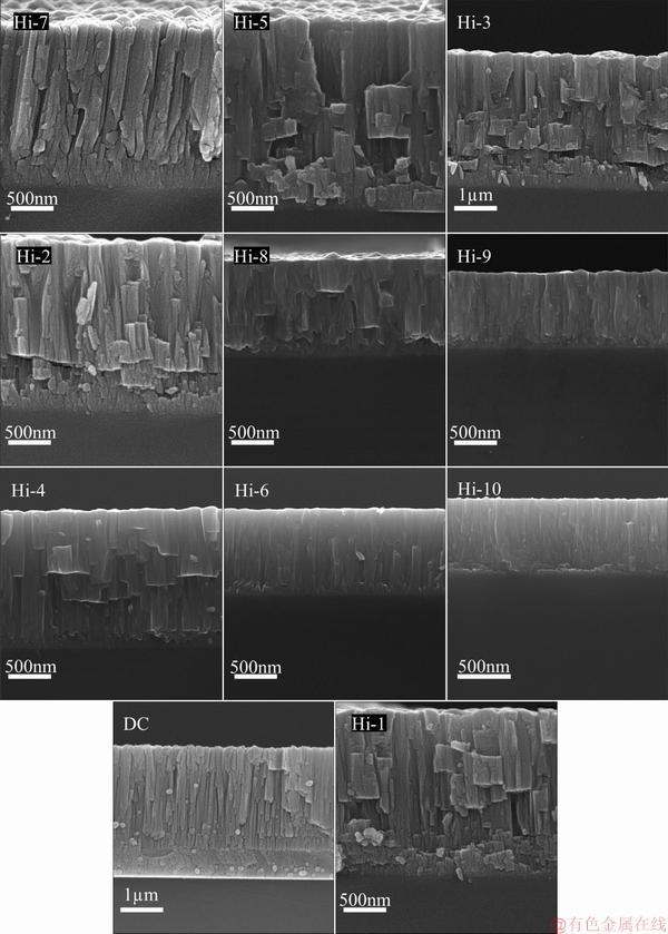
Fig. 8 FESEM cross-section images of titanium nitride deposited by DCMS and HiPIMS
Response surface methodology has been employed to study the effect of frequency and pulse-on time on the deposition rate of TiN layers. In order to reach the best fitting model, many different methods were tested, including stepwise [61,62], forward selection [63], backward selection [64,65], and box-cox transformation [66,67], with different lambda. Finally, it was observed that the box-cox transformation with optimal lambda equal to -1 and the confidence level of 95% lead to a good model fitting for predicting the deposition rate. The obtained regression equation is as follows:

 (3)
(3)
where RD is deposition rate, f is frequency and ton is pulse-on time. A conventional way to check the accuracy of a model is R2 which is calculated for this model. The R2, R2 (adjusted), and R2 (prediction) are 99.95%, 99.91%, and 99.33%, respectively, proving that the model is of high accuracy. The R2 (prediction), which shows the capability of the model to predict new observation, is very good and this means that the model can be used for predicting other experimental results. The fitted value as well as the prediction interval for experiments are extracted from the mentioned model and are listed in Table 4. Based on the statistical analysis, the Sample Hi-3 is an outlier. Note that we repeated Hi-3 twice and although the current waveforms did not change, the deposition rate was not consistent. Therefore, it was removed from the model fitting in order to reach a rational model. Figure 10 shows the deposition rate dependency on pulse-on time and frequency according to Eq. (3). As distinctive in Fig. 10, there is an optimum in deposition rate equal to (17��0.8) nm/min where the frequency and pulse-on time are 537 Hz and 212 ��s, respectively, and the duty cycle is equal to 11.3% which is not the utmost value. Although it is usually assumed that by increasing the duty cycle, the deposition rate increases [68], the analyses say that the maximum deposition rate is at a point that the duty cycle is not the maximum. Note that the deposition rate is dependent on the sputtering rate, transferring the sputtered atoms or ions to the substrate as well as the real-time of the process. When the duty cycle is low, normally the peak power (or the current) is high, so the sputtering rate is also high but at the expense of the real-time of sputtering. When the real-time (duty cycle) increases, approaching the DCMS process, the power and the sputtering rate are low, supporting less amount of atoms or ions for the deposition. Hence, it seems that there is an optimum point at which the effect of real-time and sputtering rate leads to a maximum amount of metal ions and atoms reaching the substrate.
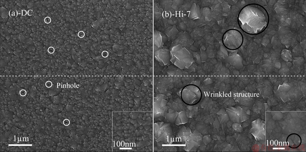
Fig. 9 FESEM images from top of titanium nitride layers deposited by DCMS (a) and HiPIMS (b)
Table 4 Real, fitted value and prediction interval of deposition rate of HiPIMS and DCMS

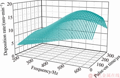
Fig. 10 Deposition rate (according to Eq. (3)) in terms of deposition parameters (frequency and pulse-on time) of HiPIMS
ANOVA is widely used to test the significance of the regression, which, here, is carried out for the deposition rate, and the obtained data are listed in Table 5. In this table, DF is the degree of freedom, the F-value is the mean regression sum of squares over the mean error sum of squares, and P-value shows the probability of accepting the null hypothesis. In other words, the low P-value means that the probability to reject the null hypothesis is high and the given term is significant. As seen in Table 5, the P-value for all terms is 0.000, implying that all parameters are influential in the fitted model. Besides, the P-value for lack-of-fit is 0.107 that is larger than the value of confidence interval, ��, which is 0.05. This means that lack-of-fit for this model is negligible and for this term, there is no strong evidence against the null hypothesis. It is crucial for a good model with even very high R2, to have the P-value of the lack-of-fit more than the confidence level. Otherwise, the model is not able to predict other observations correctly. Many models were generated in this work that the value of R2 was more than 99%, however, the P-value for lack-of-fit was less than 0.05, showing the inaccuracy of the model to predict. In order to make the model appropriate, the outlier data, Hi-3, was removed from the analysis, resulting in a model statistically and based on the R2 and P-value of lack-of-fit to be acceptable.
Table 5 Results of ANOVA for deposition rate
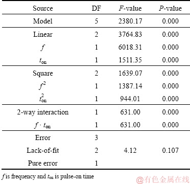
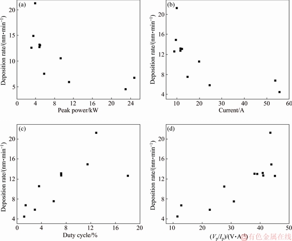
Fig. 11 Effect of peak power (a), current (b), duty cycle (c) and voltage/current (d) on deposition rate of TiN with HiPIMS
Although the experiments were designed in terms of frequency and pulse-on time, the obtained results are plotted versus other parameters including the peak power, peak current, duty cycle, and peak voltage divided by peak current (Vp/Ip), as depicted in Fig. 11. As seen, when the peak power and peak current increase, (Figs. 11(a, b)), the deposition rate is generally low. Besides, it should be noted that the average power for all tests is equal to 250 W. When the current increases, although more ions reach the substrate, the sputtering of the deposited layer could occur, which leads to the lower deposition rate but denser and harder coatings. In Fig. 11(c), it is shown that when the duty cycle increases, the deposition rate almost increases. Since the duty cycle is related to the real-time of deposition, the more duty cycle means the more real-time of the process. Therefore, it is logical that the deposition rate increases when the duty cycle is higher. However, as seen in Fig. 11(c), it decreases when the duty cycle goes beyond 15% that could be linked to the current waveforms. In Fig. 11(d), the deposition rate versus peak voltage/peak current (Vp/Ip) is drawn. It is intriguing to notice that Vp/Ip, as mentioned in Section 3.1, is linked to the impedance of the plasma. This figure shows that the higher the Vp/Ip or impedance, the higher the deposition rate is.
4 Conclusions
(1) The simultaneous effect of two key factors in HiPIMS, namely, frequency (162-637 Hz) and pulse-on time (37-322 ��s) was explored on both the current waveforms and the layer properties such as crystallite size, preferred orientation, microstructure, and deposition rate, which was analyzed by response surface methodology (RSM).
(2) As the crystallographic orientation and crystallite size of the HiPIMS samples were quite similar, the statistical approach was not applicable and only compared to the DCMS sample. As expected, the HiPIMS samples are quite denser with (200) preferred orientation with finer crystallite size (around 10 nm).
(3) Since the deposition rate of HiPIMS samples was noticeably linked to the frequency and pulse-on time, the statistical approach was plausible. Regression model and analyses of variance (ANOVA) showed that the deposition rate is meaningfully dependent on frequency and pulse-on time. The most interesting thing is that there is a middle area in the studied range in which the deposition rate is maximum. In other words, by increasing the pulse-on time (approaching the DCMS), the deposition rate does not necessarily increase; the highest deposition rate equal to (17��0.8) nm/min could be reached when the frequency is 537 Hz in the range of 162-637 Hz and pulse-on time is 212 ��s in the range of 37-322 ��s. This implies that the maximum deposition rate of HiPIMS could be achieved by regulating the pulse-on time and frequency into an optimum value where the quality of coatings remains intact. This finding is verified by experimental test at the optimum condition and results in a deposition rate of 16.7 nm/min.
References
[1] PRADHAN S, NOUVEAU C, VASIN A, DJOUADI M A. Deposition of CrN coatings by PVD methods for mechanical application [J]. Surface and Coatings Technology, 2005, 200: 141-145.
[2] KHAMSEH S, ARAGHI H. A study of the oxidation behavior of CrN and CrZrN ceramic thin films prepared in a magnetron sputtering system [J]. Ceramics International, 2016, 42: 9988-9994.
[3] DORCIOMAN G, SOCOL G, CRACIUN D, ARGIBAY N, LAMBERS E, HANNA M, TAYLOR C, CRACIUN V. Wear tests of ZrC and ZrN thin films grown by pulsed laser deposition [J]. Applied Surface Science, 2014, 306: 33-36.
[4] CHOU W J, YU G P, HUANG J H. Mechanical properties of TiN thin film coatings on 304 stainless steel substrates [J]. Surface and Coatings Technology, 2002, 149: 7-13.
[5] PETROV I, HULTMAN L, HELMERSSON U, SUNDGREN J E, GREENE J. Microstructure modification of TiN by ion bombardment during reactive sputter deposition [J]. Thin Solid Films, 1989, 169: 299-314.
[6] FARHADIZADEH A R, AMADEH A A, GHOMI H. The effect of metal transition dopant on electronic and mechanical properties of titanium nitride: First principle method [J]. Computational Materials Science, 2018, 141: 82-90.
[7] MEI H J, ZHAO S S, CHEN W, WANG Q M, LIANG H F. Microstructure and residual stress of TiN films deposited at low temperature by arc ion plating [J]. Transactions of Nonferrous Metals Society of China, 2018, 28: 1368-1376.
[8] WARCHOLINSKI B, GILEWICZ A, KUPRIN A S, KOLODIY I V. Structure and properties of CrN coatings formed using cathodic arc evaporation in stationary system [J]. Transactions of Nonferrous Metals Society of China, 2019, 29: 799-810.
[9] LIM J W, PARK H S, PARK T H, LEE J J, JOO J. Mechanical properties of titanium nitride coatings deposited by inductively coupled plasma assisted direct current magnetron sputtering [J]. Journal of Vacuum Science & Technology A: Vacuum, Surfaces, and Films, 2000, 18: 524-528.
[10] MUSIL J, KADLEC S, VYSKOCIL J, VALVODA V. New results in dc reactive magnetron deposition of TiNx films [J]. Thin Solid Films, 1988, 167: 107-120.
[11] TIRON V, VELICU I L, CRISTEA D, LUPU N, STOIAN G, MUNTEANU D. Influence of ion-to-neutral flux ratio on the mechanical and tribological properties of TiN coatings deposited by HiPIMS [J]. Surface and Coatings Technology, 2018, 352: 690-698.
[12] CUI W F, NIU F J, TAN Y L, QIN G W. Microstructure and tribocorrosion performance of nanocrystalline TiN graded coating on biomedical titanium alloy [J]. Transactions of Nonferrous Metals Society of China, 2019, 29: 1026-1035.
[13] GHASEMI S, FARHADIZADEH A R, AMADEH A A, GHOMI H. Structural and morphological properties of TiN deposited by magnetron sputtering [J]. Surface Topography: Metrology and Properties, 2018, 6(4): 045003-045018.
[14] JITHIN M, KOLLA L G, VIKRAM G, UDAYASHANKAR N, MOHAN S. Pulsed DC magnetron sputtered titanium nitride thin films for localized heating applications in MEMS devices [J]. Sensors and Actuators A: Physical, 2018, 272: 199-205.
[15] GUDMUNDSSON J T, ALAMI J, HELMERSSON U. Spatial and temporal behavior of the plasma parameters in a pulsed magnetron discharge [J]. Surface and Coatings Technology, 2002, 161: 249-256.
[16] KOUZNETSOV V, MACAK K, SCHNEIDER J M, HELMERSSON U, PETROV I. A novel pulsed magnetron sputter technique utilizing very high target power densities [J]. Surface and Coatings Technology, 1999, 122: 290-293.
[17] EHIASARIAN A, NEW R, M��NZ W D, HULTMAN L, HELMERSSON U, KOUZNETSOV V. Influence of high power densities on the composition of pulsed magnetron plasmas [J]. Vacuum, 2002, 65: 147-154.
[18] SARAKINOS K, ALAMI J, KONSTANTINIDIS S. High power pulsed magnetron sputtering: A review on scientific and engineering state of the art [J]. Surface and Coatings Technology, 2010, 204: 1661-1684.
[19] HELMERSSON U, LATTEMANN M, BOHLMARK J, EHIASARIAN A P, GUDMUNDSSON J T. Ionized physical vapor deposition (IPVD): A review of technology and applications [J]. Thin Solid Films, 2006, 513: 1-24.
[20] BISWAS B, PURANDARE Y, SUGUMARAN A, KHAN I, HOVSEPIAN P E. Effect of chamber pressure on defect generation and their influence on corrosion and tribological properties of HIPIMS deposited CrN/NbN coatings [J]. Surface and Coatings Technology, 2018, 336: 84-91.
[21] DING J C, WANG Q M, LIU Z R, JEONG S, ZHANG T F, KIM K H. Influence of bias voltage on the microstructure, mechanical and corrosion properties of AlSiN films deposited by HiPIMS technique [J]. Journal of Alloys and Compounds, 2019, 772: 112-121.
[22] HAYE E, COLAUX J L, MOSKOVKIN P, PIREAUX J J, LUCAS S. Wide range investigation of duty cycle and frequency effects on bipolar magnetron sputtering of chromium nitride [J]. Surface and Coatings Technology, 2018, 350: 84-94.
[23] GANESAN R, AKHAVAN B, DONG X, MCKENZIE D R, BILEK M M M. External magnetic field increases both plasma generation and deposition rate in HiPIMS [J]. Surface and Coatings Technology, 2018, 352: 671-679.
[24] WU Z, XIAO S, MA Z, CUI S, JI S, TIAN X, FU R K, CHU P K, PAN F. Discharge current modes of high power impulse magnetron sputtering [J]. AIP Advances, 2015, 5: 097178.
[25] GUDMUNDSSON J T, BRENNING N, LUNDIN D, HELMERSSON U. High power impulse magnetron sputtering discharge [J]. Journal of Vacuum Science & Technology A: Vacuum, Surfaces, and Films, 2012, 30: 030801.
[26] MAGNUS F, SVEINSSON O B, OLAFSSON S, GUDMUNDSSON J T. Current-voltage-time characteristics of the reactive Ar/N2 high power impulse magnetron sputtering discharge [J]. Journal of Applied Physics, 2011, 110: 083306.
[27] CLARKE G, MISHRA A, KELLY P J, BRADLEY J W. Cathode current density distributions in high power impulse and direct current magnetron sputtering modes [J]. Plasma Processes and Polymers, 2009, 6(S): s548-s553.
[28] ANDERS A, ANDERSSON J, EHIASARIAN A. High power impulse magnetron sputtering: Current-voltage-time characteristics indicate the onset of sustained self-sputtering [J]. Journal of Applied Physics, 2007, 102: 113303.
[29] HUO C, LUNDIN D, RAADU M A, ANDERS A, GUDMUNDSSON J T, BRENNING N. On the road to self- sputtering in high power impulse magnetron sputtering: Particle balance and discharge characteristics [J]. Plasma Sources Science and Technology, 2014, 23: 025017.
[30] ZHAO X, JIN J, CHENG J C, LEE J W, WU K H, LIU K C. Effect of pulsed off-times on the reactive HiPIMS preparation of zirconia thin films [J]. Vacuum, 2015, 118: 38-42.
[31] WU B, HAEHNLEIN I, SHCHELKANOV I, MCLAIN J, PATEL D, UHLIG J, JURCZYK B, LENG Y, RUZIC D N. Cu films prepared by bipolar pulsed high power impulse magnetron sputtering [J]. Vacuum, 2018, 150: 216-221.
[32] CHANG C L, SHIH S G, CHEN P H, CHEN W C, HO C T, WU W Y. Effect of duty cycles on the deposition and characteristics of high power impulse magnetron sputtering deposited TiN thin films [J]. Surface and Coatings Technology, 2014, 259: 232-237.
[33] FERREIRA F, SERRA R, OLIVEIRA J C, CAVALEIRO A. Effect of peak target power on the properties of Cr thin films sputtered by HiPIMS in deep oscillation magnetron sputtering (DOMS) mode [J]. Surface and Coatings Technology, 2014, 258: 249-256.
[34] LI G, SUN J, XU Y, XU Y, GU J, WANG L, HUANG K, LIU K, LI L. Microstructure, mechanical properties, and cutting performance of TiAlSiN multilayer coatings prepared by HiPIMS [J]. Surface and Coatings Technology, 2018, 353: 274-281.
[35] BOX G E, WILSON K B. On the experimental attainment of optimum conditions [J]. Journal of the Royal Statistical Society: Series B (Methodological), 1951, 13: 1-38.
[36] WANG X, BAI S, LI F, LI D, ZHANG J, TIAN M, ZHANG Q, TONG Y, ZHANG Z, WANG G. Effect of plasma nitriding and titanium nitride coating on the corrosion resistance of titanium [J]. The Journal of Prosthetic Dentistry, 2016, 116: 450-456.
[37] WU C K, HUANG J H, YU G P. Optimization of deposition processing of VN thin films using design of experiment and single-variable (nitrogen flow rate) methods [J]. Materials Chemistry and Physics, 2019, 224: 246-256.
[38] WANG L, LI L, KUANG X. Effect of substrate bias on microstructure and mechanical properties of WC-DLC coatings deposited by HiPIMS [J]. Surface and Coatings Technology, 2018, 352: 33-41.
[39] ROSSNAGEL S, KAUFMAN H. Current�Cvoltage relations in magnetrons [J]. Journal of Vacuum Science & Technology A: Vacuum, Surfaces, and Films, 1988, 6: 223-229.
[40] CAPEK J, HALA M, ZABEIDA O, KLEMBERG-SAPIEHA J E, MARTINU L. Steady state discharge optimization in high-power impulse magnetron sputtering through the control of the magnetic field [J]. Journal of Applied Physics, 2012, 111: 023301.
[41] YUSHKOV G Y, ANDERS A. Origin of the delayed current onset in high-power impulse magnetron sputtering [J]. IEEE Transactions on Plasma Science, 2010, 38: 3028-3034.
[42] MUSIL J, LESTINA J, VLCEK J, TOLG T. Pulsed dc magnetron discharge for high-rate sputtering of thin films [J]. Journal of Vacuum Science & Technology A: Vacuum, Surfaces, and Films, 2001, 19: 420-424.
[43] THORNTON J A. Magnetron sputtering: Basic physics and application to cylindrical magnetrons [J]. Journal of Vacuum Science and Technology, 1978, 15: 171-177.
[44] WAITS R K. Planar magnetron sputtering [J]. Journal of Vacuum Science and Technology, 1978, 15: 179-187.
[45] ROSSNAGEL S, KAUFMAN H. Charge transport in magnetrons [J]. Journal of Vacuum Science and Technology A: Vacuum, Surfaces, and Films, 1987, 5: 2276-2279.
[46] ALAMI J, SARAKINOS K, MARK G, WUTTIG M. On the deposition rate in a high power pulsed magnetron sputtering discharge [J]. Applied Physics Letters, 2006, 89: 154104.
[47] ANDERS A. Fundamentals of pulsed plasmas for materials processing [J]. Surface and Coatings Technology, 2004, 183: 301-311.
[48] ANDERS A. Self-sputtering runaway in high power impulse magnetron sputtering: The role of secondary electrons and multiply charged metal ions [J]. Applied Physics Letters, 2008, 92: 201501.
[49] VASU K, KRISHNA M G, PADMANABHAN K A. Substrate-temperature dependent structure and composition variations in RF magnetron sputtered titanium nitride thin films [J]. Applied Surface Science, 2011, 257: 3069-3074.
[50] BARAGIOLA R A, ALONSO E V, FERRON J, OLIVA-FLORIO A. Ion-induced electron emission from clean metals [J]. Surface Science, 1979, 90: 240-255.
[51] CHAWLA V, JAYAGANTHAN R, CHANDRA R. Structural characterizations of magnetron sputtered nanocrystalline TiN thin films [J]. Materials Characterization, 2008, 59: 1015-1020.
[52] ARSHI N, LU J, JOO Y K, LEE C G, YOON J H, AHMED F. Study on structural, morphological and electrical properties of sputtered titanium nitride films under different argon gas flow [J]. Materials Chemistry and Physics, 2012, 134: 839-844.
[53] PETROV I, MYERS A, GREENE J E, ABELSON J R. Mass and energy resolved detection of ions and neutral sputtered species incident at the substrate during reactive magnetron sputtering of Ti in mixed Ar+N2 mixtures [J]. Journal of Vacuum Science and Technology A: Vacuum, Surfaces, and Films, 1994, 12: 2846-2854.
[54] EHIASARIAN A P, GONZALVO Y A, WHITMORE T D. Time-resolved ionisation studies of the high power impulse magnetron discharge in mixed argon and nitrogen atmosphere [J]. Plasma Processes and Polymers, 2007, 4(S): s309-s313.
[55] EHIASARIAN A P, VETUSHKA A, GONZALVO Y A, SAFRAN G, SZEKELY L, BARNA P B. Influence of high power impulse magnetron sputtering plasma ionization on the microstructure of TiN thin films [J]. Journal of Applied Physics, 2011, 109: 104314.
[56] SUBRAMANIAN B, ASHOK K, SUBRAMANIAN K, SASTIKUMAR D, SELVAN G, JAYACHANDRAN M. Evaluation of corrosion and wear resistance titanium nitride (TiN) coated on mild steel (MS) with brush plated nickel interlayer [J]. Surface Engineering, 2013, 25: 490-495.
[57] BISWAS B, PURANDARE Y, KHAN I, HOVSEPIAN P E. Effect of substrate bias voltage on defect generation and their influence on corrosion and tribological properties of HIPIMS deposited CrN/NbN coatings [J]. Surface and Coatings Technology, 2018, 344: 383-393.
[58] BANERJEE T, CHATTOPADHYAY A. Influence of substrate bias on structural and tribo-mechanical properties of pulsed magnetron sputtered TiN-WSx hard-lubricious coating [J]. Tribology International, 2018, 123: 81-91.
[59] BAUMANN F, CHOPP D, de la RUBIA T D, GILMER G, GREENE J, HUANG H, KODAMBAKA S, O'SULLIVAN P, PETROV I. Multiscale modeling of thin-film deposition: Applications to Si device processing [J]. MRS Bulletin, 2001, 26: 182-189.
[60] GREENE J E, SUNDGREN J E, HULTMAN L, PETROV I, BERGSTROM D B. Development of preferred orientation in polycrystalline TiN layers grown by ultrahigh vacuum reactive magnetron sputtering [J]. Applied Physics Letters, 1995, 67: 2928-2930.
[61] YU L, DAS P K, ZHENG Y. Stepwise response surface method and its application in reliability analysis of ship hull structure [J]. Journal of Offshore Mechanics and Arctic Engineering, 2002, 124: 226-230.
[62] MENG X J, JING S K, ZHANG L X, LIU J H, YANG H C. A new sampling approach for response surface method based reliability analysis and its application [J]. Advances in Mechanical Engineering, 2015, 7: 305473.
[63] ROUSSOULY N, PETITJEAN F, SALAUN M. A new adaptive response surface method for reliability analysis [J]. Probabilistic Engineering Mechanics, 2013, 32: 103-115.
[64] OWCZAREK A, KUZMA L, WYSOKINSKA H, OLSZEWSKA M A. Application of response surface methodology for optimisation of simultaneous UHPLC-PDA determination of oleanolic and ursolic acids and standardisation of Ericaceae medicinal plants [J]. Applied Sciences, 2016, 6: 244-259.
[65] ORHAN G, HAPC G, KELES O. Application of response surface methodology (RSM) to evaluate the influence of deposition parameters on the electrolytic Cu-Zn alloy powder [J]. Int J Electrochem Sci, 2011, 6: 3966-3981.
[66] BHARDWAJ B, KUMAR R, SINGH P K. An improved surface roughness prediction model using Box-Cox transformation with RSM in end milling of EN 353 [J]. Journal of Mechanical Science and Technology, 2014, 28: 5149-5157.
[67] BHARDWAJ B, KUMAR R, SINGH P K. Surface roughness (Ra) prediction model for turning of AISI 1019 steel using response surface methodology and Box�CCox transformation [J]. Proceedings of the Institution of Mechanical Engineers, Part B: Journal of Engineering Manufacture, 2014, 228: 223-232.
[68] BRADLEY J W, MISHRA A, KELLY P J. The effect of changing the magnetic field strength on HiPIMS deposition rates [J]. Journal of Physics D: Applied Physics, 2015, 48: 215202.
Saeed GHASEMI, Ali Reza FARHADIZADEH, Hamid GHOMI
Laser and Plasma Research Institute, Shahid Beheshti University, Evin 1983963113, Tehran, Iran
ժ Ҫ�����ô�������ſؽ���(HiPIMS)���ڲ�ͬƵ��(162~637 Hz)������ʱ��(60~322 ��s)�����£��������ѱ�Ĥ�����ڹ�����ϡ�������Ӧ�淨�о�Ƶ�ʺ�����ʱ��Ե������Ρ�����ȡ������֯��ЭͬӰ�죬�ر��ǶԺ㶨ʱ�䡢ƽ������Ϊ250 W�����µ����ѳ������ʵ�Ӱ�졣�ֱ���XRD��FESEM�Գ�����Ĥ�ľ���ṹ����ò���з����������������Ʒ�ij�������������ʱ�������Ƶ���кܴ�Ĺ�ϵ������������4.5~14.5 nm/min֮��仯���ع鷽�̺ͷ��������ʾ����Ƶ��Ϊ537 Hz������ʱ��Ϊ212 ��sʱ�������������Ϊ(17��0.8) nm/min��ʵ��������ô������µij�������Ϊ16.7 nm/min����Ԥ��ֵ�ǺϽϺá�
�ؼ��ʣ���������ſؽ���(HiPIMS)�������ѣ���Ӧ�淨(RSM)���������ʣ��������
(Edited by Bing YANG)
Corresponding author: Hamid GHOMI; Tel: +98-2129903072; E-mail: h-gmdashty@sbu.ac.ir
DOI: 10.1016/S1003-6326(19)65165-4

