Electrical Conductivity of Ce-Nd Co-doped SnO2 Based on the First-Principle
Yu Shuangmiao Wang Jingqin Chen Ling Liu Zhou
State Key Laboratory of Reliability and Intelligence of Electrical Equipment,Hebei University of Technology
Key Laboratory of Electromagnetic Field and Electrical Apparatus Reliability of Hebei Province,Hebei University of Technology
Abstract��
The new AgSnO2 material is the most suitable electrical contact material for replacing AgCdO material. But AgSnO2 electrical contact would precipitate SnO2 crystals on its surface during use. The conductivity of SnO2 is extremely poor,which affects the use of electrical contacts seriously. How to improve the electrical conductivity of SnO2 has become the main direction of scholars' research.This research adopted the first principle based on density functional theory,and aimed to simulate and analyse the effects of co-doping Ce and Nd with SnO2 on energy band diagrams,state densities,charge distribution and electrical conductivity. The results showed that both single-doping and co-doping could reduce the band gap of SnO2,meanwhile tightening the energy bands. Moreover,the performance of co-doping samples was noticed significantly better than that of single-doping samples. The 4 f state of Nd atoms and Ce atoms during single doping introduced a new impurity level at the bottom of the SnO2 conduction band. The conduction band bottom moved toward the lower energy level. On the other hand,when Ce and Nd were co-doped,more energy levels were introduced to the conduction band bottom and the valence band top of SnO2,which further shortened the band gap. Furthermore,by the assistance of layout charge analysis,it was identified that the ionicity of the co-doped sample was stronger than that of the single-doped sample. Most importantly,both single doping and co-doping could contribute to the increase of electrical conductivity of SnO2 electrical conduction materials,and the effectiveness of co-doping was significantly higher than those of single doping.
Keyword��
electrical contact materials;first principles;SnO2;rare earth element co-doping;electrical properties;
Received�� 2019-04-08
����ĵ紥ͷ����Ӧ�������õĵ����ԡ������ԡ����ۺ��ԡ�������ת�ơ����绡��ʴ�����Լ��Ͷ��ȶ��ĽӴ�����
[1]�������������Ƕ�ʹ��Ag Cd O��Ϊ��ͷ���ϵ���Ҫ�ɷ֣���Ϊ�����͵绡��ʴ�ԡ����ۺ��ԡ���ʴ����ĥ�Եȷ���������������ܣ���һ�ȱ���Ϊ�����ܡ��Ĵ�ͷ���ϡ����ǽ����������ǶԻ��������Ͱ�ȫ�����ӳ̶�Խ��Խ�ߣ���Ag Cd O��ͷ������ʹ�ù����в�����Cd�������о綾�ģ�ͬʱҲ��Ի����������ص���Ⱦ�����Ag Cd O������������̭
[2,3]��
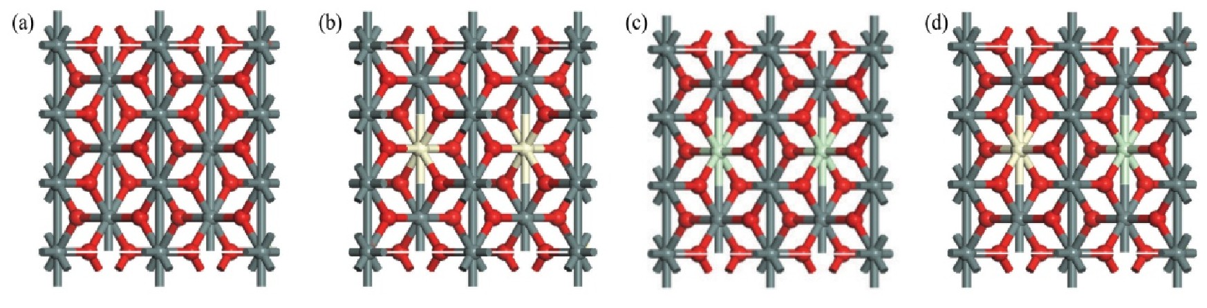
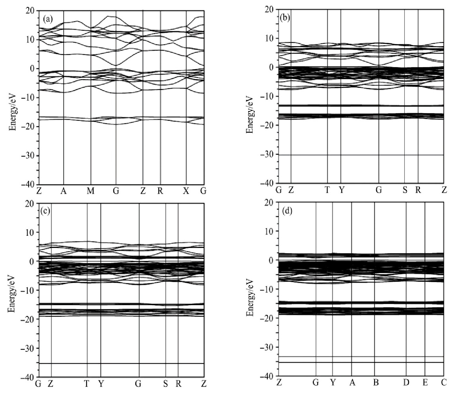
����Sn O2����������ϵSn O2���ܴ��ṹͼ��ͼ2��ʾ����ͼ2(a����֪����Sn O2�������Ӻ��Sn O2ģ�͵ĵ����ͼ۴�����λ�ڲ���Ԩ����G�㣬�����Ƕ���ֱ�Ӵ�϶�뵼�塣���б���Sn O2�Ĵ�϶����ֵΪ1.1 e V�����Ǹü���ֵ����С��ʵ��ֵ3.6 e V
[17]���������ڼ���ģ����ʹ�õĹ����ݶȽ��ƴ���һ�������ԣ���Ҫ�ǵ���Sn��5s��5p̬��O��2p̬֮�����ų����ã�ʹ�ü���ֵ��ƫС�����ڱ�ʵ�鿼�ǶԱȸ���������ϵ�Ĵ�϶��Դ�С����ʵ����۲����ܵ�Ӱ�졣
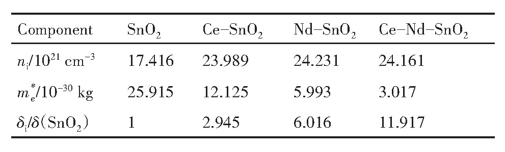
�������㣬ϡ������Sn O2�Ĵ�϶�ֱ�Ϊ��CeSn O2Ϊ0.805 e V,Nd-Sn O2Ϊ0.736 e V,Ce-Nd-Sn O2Ϊ0.701 e V��ͨ����������֪��������ϡ��Ԫ�غ�Sn O2��϶���Ⱦ�������С����Ce,Nd������Sn O2��ϵ�Ĵ�϶���Ƚ�һ����С����һ���̶��Ͽ��Ա���Ce,Nd������Sn O2�ĵ����Ը�ǿ�����ܴ�ͼ2(b��d������ֱ�۵ؿ������Ӻ��ͼ۴�����ø��ӽ��ܣ��ҳ������µļ۴����������������ƶ�������������ϵ���ܴ�ͼ��Ϊ������ƽ�����䵼�����������ƶ��ɶ�Ҫǿ�ڵ�����ϵ���������ӿ��������ܼ������۴�Ҳ���������ƶ��������ͼ۴������ܴ���ʮ���ܼ���������۴������������ܼ����뵼�巢�������ָ�ǿ�Ľ����ԣ�ʹ��������ǿ��
ͼ3��ʾΪ�������õı���Sn O2,Ce�����ӣ�Nd�����Ӻ�Ce,Nd������Sn O2��ϵ����̬�ܶ�ͼ�ͷ�̬�ܶ�ͼ���ۺ�ͼ3(a��d���ɷ�����֪�����ڱ���Sn O2���䵼��λ��0��20 e V�䣬��Ҫ��Snԭ�ӵ�5s,5p̬��ͬ�ṩ�����۴�������������ֵ���ϼ۴�λ��-10��0 e V����Snԭ�ӵ�5s,5p̬��Oԭ�ӵ�2p̬��ͬ�ṩ���¼۴�λ��-20��-15 e V����Oԭ�ӵ�2s̬��Snԭ�ӵ�5s,5p̬�ṩ����CeԪ�ص�����ʱ����������λ��0��10 e V��������Ceԭ�ӵ�4f̬��Snԭ�ӵ�5s̬��ͬ��ɣ�����Ce��4f̬Ϊ��Ҫ��ɳɷ֣�Sn��5s,5p̬����ܴ����ƶ������۴�����λ��-10��0 e V��Զ������ܼ��IJ��ֶԷ����ܼ���Ӱ��ɺ��Բ��ƣ��۴���Ҫ��Snԭ�ӵ�5s,5p̬��Oԭ��2p̬��ͬ�ṩ����NdԪ�ص�����ʱ������λ��0��10 e V��������Ndԭ�ӵ�4f̬��Snԭ�ӵ�5s,5p̬��ͬ�ṩ������Nd��4f̬Ϊ��Ҫ��ɳɷ֣�Sn��5s,5p̬����ܶ��ƶ������۴�λ��-10��0 e V��Զ������ܼ��IJ��ֺ��Բ��ƣ��۴���Ҫ��Snԭ�ӵ�5s,5p̬��Oԭ�ӵ�2p̬��Ndԭ�ӵ�4f̬��ͬ�ṩ����Ce,Nd������ʱ������λ��0��5 e V��������Ceԭ�ӵ�4f̬��Ndԭ�ӵ�4f̬��Snԭ�ӵ�5s̬��ͬ�ṩ������Ceԭ�ӵ�4f̬��Ndԭ�ӵ�4f̬Ϊ��Ҫ��ɳɷ֣�Snԭ�ӵ�5s,5p̬����������ܶ��ƶ������۴�λ�ڨC10��0 e V��Զ������ܼ����ֺ��Բ��ƣ��۴���Snԭ�ӵ�5s,5p̬��Oԭ�ӵ�2p̬��Ndԭ�ӵ�4f̬��ͬ�ṩ������Oԭ�ӵ�2p̬Ϊ��Ҫ�ɷ֡�