文章编号:1004-0609(2007)05-0727-05
基于氧化铝模板直接电沉积法镍纳米线的制备与表征
于 美,刘建华,李松梅
(北京航空航天大学 材料科学与工程学院, 北京 100083)
摘 要:在未氧化铝和氧化铝之间经过降压剪薄阻挡层直接进行电沉积,采用不同电压进行电沉积制备了镍纳米线,并采用SEM,TEM和X射线衍射对所制备的镍纳米线进行了表征,研究了电沉积电压对纳米线结构的影响。结果表明:镍纳米线的外形决定于氧化铝模板的形貌,其直径和最大长度分别依赖于模板孔洞的直径和长度,当电沉积电压为1,1.5和2 V时制备的镍纳米线为多晶结构,随着电沉积电压的升高,镍纳米线为沿[220]择优取向的单晶结构(电沉积电压分别为3 V和4 V),当电沉积电压进一步升高时,择优取向由[220]转为[111]方向(电沉积电压5 V)。
关键词:镍纳米线;氧化铝模板;电沉积;晶体结构
中图分类号:O 614 文献标识码:A
Preparation and characterization of nickel nanowires by direct electrodeposition in anodic alumina membrane
YU Mei, LIU Jian-hua, LI Song-mei
(School of Materials Science and Engineering, Beijing University of Aeronautics and Astronautics, Beijing 100083)
Abstract: The nickel nanowires were prepared directly by electrodeposition in anodic alumina membrane (AAM) after modification of AAM. The structure and topography of nanowires were characterized by SEM, TEM and XRD. The effect of deposition voltage on texture of nickel nanowires was studied. The results show that the morphologies of nickel nanowires depend on anodic alumina membrane. The diameter and length of nanowires are separately affected by pore diameter of AAM and deposition time. The nickel nanowires are poly-crystalline when the deposition voltages are low, such as 1 V, 1.5 V and 2 V. The nickel nanowires change to single crystal with a preferred orientation along [220] when the depositon voltages become larger, such as 3 V and 4 V. The preferred orientation transforms from [220] to [111] with further increase of deposition voltage (5 V).
Key words: nickel nanowires; anodic alumina membrane; electrodeposition; crystalline structure
一维纳米材料具有优异的物理和化学性能,其制备方法引起了各国科学家的注意,其中模板法是一种能够实现纳米线可控生长的重要制备方法[1-3]。目前,已经用模板法制备出多种材料的纳米线,如Au,Ag,Fe,Co和Cu等金属、合金[2-5]及ZnO和Fe2O3等氧化物[6-8]。这些材料的制备一般采用溶胶-凝胶法[6-7]、无电电沉积[9]、直流电沉积[8]、交流电沉积[10]、化学镀[3]、脉冲电沉积[4]和化学气相沉积(CVD)[11]等。其中是由于电沉积具有方法简单、制备的纳米线填充度高及长径比可控等优点得到了广泛的应用[8]。交流电沉积所制备的纳米线微观结构会出现堆垛和重叠,影响纳米线的结晶程度,使得脉冲电沉积操作繁琐,因此电沉积中又以直流电沉积应用更为广泛。由于该模板含有氧化铝层与未氧化铝层之间的不导电致密阻挡 层[12],因此目前进行电沉积最主要的方法是先除去未氧化的铝,再除去阻挡层,然后再在穿孔的氧化铝模板一侧喷覆金、铂、铜等金属,作为导电层进行电沉积。这样不仅增加了研究的成本和繁琐度,且在穿孔过程中导致氧化铝模板孔洞的直径难以控制。
镍是具有高熔点的铁磁性金属,具有良好的磁学性能[3],做为二次电池的电极也表现出优良的性能。潘谷平等[1]采用交流电沉积法制备了多晶镍纳米线,并对其电磁性能和电化学性能进行了研究。Pan等[3]对制备镍纳米线的电沉积电压以及温度对晶体结构的影响进行了研究,并研究了其结构对其磁性性能的影响。结果发现,低温下高电沉积电压时可以制备出单晶镍纳米线,纳米线沿[220]择优生长,单晶镍纳米线具有更高的矫顽力、更大的磁化面积和更为显著的各向异性。关于择优取向对材料磁性性能的影响也有报道,Hu等[13]利用氧化铝模板法制备了铁纳米线,通过调整电沉积过程中的pH值,制备了择优取向分别为[110]和[200]的铁纳米线,并对其磁性能进行了测试,结果发现沿[200]择优取向的铁纳米线具有更大的矩形度和矫顽力。
综上所述,材料的结构会对材料的性能产生很大的影响。虽然金属镍纳米线的氧化铝模板法制备已经有过较多报道,但并没有通过简单的改变电沉积电压直接制备出单晶择优取向不同的镍纳米线的报道。本文作者在未氧化的铝层和氧化铝层间采用降压剪薄阻挡层直接电沉积方法制备了镍纳米线,并对不同电压对电沉积镍纳米线晶体结构的影响进行了研究。随着电沉积电压的改变,镍纳米线的晶体结构发生改变,先是由多晶变成沿[220]择优取向的单晶,随着电压的进一步升高,择优取向发生了改变,变为沿[111]择优取向。这种晶体结构的不同,可能会对其磁学等性能产生较大的影响。
1 实验
氧化铝模板的制备采用二次阳极化法[12],其主要制备过程见文献[6]。本研究所用的氧化铝模板的制备工艺条件为室温下氧化电压40 V,电解质为0.3 mol/L草酸。第二次阳极化工艺完成以后,进行降压,降压速度为1~1.5 V/s,直至降为1 V,冲洗,进行电沉积制备镍纳米线。以所制备的氧化铝模板为阴极,纯镍板为阳极,室温下进行电沉积。电沉积溶液为硫酸镍200 g/L,氯化镍50 g/L,硼酸45 g/L,pH值为4.4~5.2。在室温下采用电沉积电压分别为1.0,1.5,2.0,3.0,4.0和5.0 V研究了电沉积电压对镍纳米线结构的影响。
分别用扫描电子显微镜(XL30 S-FEG,SIRION)、透射电子显微镜(H-9000 NAR HITACHI)和X射线衍射仪(D/max2200PC Cu靶,40 kV,40 mA)对镍纳米线的形貌、结构等进行了表征。在进行SEM观察以前,将6 mol/L NaOH滴加在包含镍纳米线的模板上溶解10 min,溶解完后用去离子水冲洗、干燥。在进行TEM表征以前把氧化铝模板和未氧化的铝用NaOH溶解,溶解之后用去离子水冲洗,用微栅铜网捞取一部分纳米线进行观察。
2 结果与讨论
图1所示为氧化铝模板孔径约为50 nm,室温,电沉积电压为5 V电沉积时间为15 min时制备的镍纳米线的SEM像。图1(a)所示为镍纳米线的侧面图。从图1(a)中可以看出镍纳米线平行排列,具有很好的取向性。右下部的分层是因为模板制备过程中的降压引起的。阳极氧化铝模板孔洞的孔径与阳极氧化电压成正比[7]。在降压过程中,氧化铝模板孔洞的孔径随着阳极氧化电压的降低而减小。镍纳米线的外形与氧化铝模板具有相似性,因此最终导致镍纳米线的根部分枝、变细。降压过程中镍纳米线形状和阳极氧化电流变化的详细研究见文献[14]。图1(b)所示为纳米线的俯视图。由于溶解的原因,有些完全从氧化铝模板中释放的镍纳米线堆积在一起。从图1(b)中可知,镍纳米线的直径约为50 nm,与用来进行电沉积的氧化铝模板的孔径相似。镍纳米线的直径在整个长度范围内一致,不同电压制备的电沉积镍纳米线SEM像具有共同的特征。
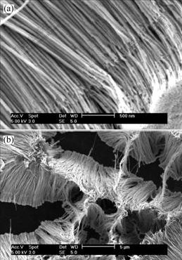
图1 镍纳米线的SEM像
Fig.1 SEM images of nickel nanowires: (a) Cross-section; (b) Large area
随着电沉积时间的延长,纳米线的长度也随之增大,最终导致超出氧化铝模板的厚度形成完整的镍层。此时模板的颜色由电沉积纳米镍所致而出现的黑色变为光亮的银灰色镍。
图2所示为室温不同电压下在孔洞直径约为50 nm的氧化铝模板中制备镍纳米线的X射线衍射谱。由图2可看出,当电压为1和1.5 V,电沉积时间为30 min;当电压为2,3,4和5 V时,电沉积时间为15 min。对照PDF870712可知,本研究中不同电沉积电压制备的镍纳米线都具有面心立方(FCC)结构。
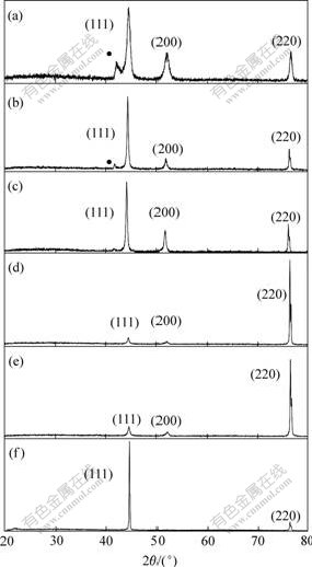
图2 室温下不同电沉积电压制备的包埋在氧化铝模板中的镍纳米线X射线衍射谱
Fig.2 XRD patterns of nickel nanowires prepared at room temperature with AAM: (a) 1 V, 30 min; (b) 1.5 V, 30 min; (c) 2 V, 15 min; (d) 3 V, 15 min; (e) 4 V, 15 min; (f) 5 V, 15 min
当电沉积电压为3和4 V时,所制备的镍纳米线在[220]方向具有择优取向;当电压为5 V时,制备的镍纳米线沿[111]择优生长。
为了进一步研究不同电沉积电压下所制备的镍纳米线的结构,对其进行了透射电镜和选区X射线衍射分析。图3所示为镍纳米的TEM像。图3(a)所示为电沉积电压为1.5 V时的单根纳米线的TEM像,插图是该纳米线的选区衍射图谱(电沉积电压为1 V和2 V时制备的镍纳米线衍射结果与此相似)。从图3中可以看出,镍纳米线的直径在长度范围内基本一致,约为50 nm,具有多晶结构。
图3(c)所示为电沉积电压为5 V时的镍纳米的TEM像,插图为该纳米线的选区衍射图,(沉积电压为3V和4V的纳米线结果与此相似)。从图3(c)中可以看出,镍纳米线具有单晶结构。图3(e)所示为纳米线的根部图,从图3(e)中可以更清楚的看到由于氧化铝模板的制备过程中降压而引起的镍纳米线根部的变细、分枝现象。图3(f)所示为大面积内镍纳米线的照片,从图3(f)中可以看出镍纳米线除根部外在整个长度范围内具有均一的直径。
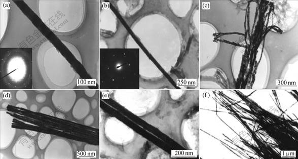
图3 镍纳米线的TEM像
Fig.3 TEM images of nickel nanowires: (a) Single nanowire, 25 ℃, 1.5 V; (b) Single nanowire, 25 ℃, 5 V; (c) Bottom of nanowires; (d) Cluster of nanowire, 25 ℃, 1.5 V; (e) Two adjacent nanowires, 25 ℃, 5 V; (f) Nanowires in large area
由透射电镜分析结果可知,室温下,低沉积电压(1, 1.5和2 V)可以制备出多晶的镍纳米线,高沉积电压可以制备出单晶镍纳米线。镍纳米线的生长从形核开始,当晶核尺寸超过临界晶核尺寸时,镍纳米线开始生长。晶粒长大过程中具有低表面能的晶粒能够迅速生长,合并其它具有高表面能的晶粒形成大晶粒成为柱状晶。温度相同时,过电位越小,临界晶核尺寸越大,随着过电位的增大,临界晶胞尺寸减小[15]。当过电位较小时,临界晶核尺寸较大,成核几率较小,晶粒间的合并较为困难,阻碍了单晶镍的生长,因此生成多晶的镍纳米线如本实验中电沉积电压为1,1.5和2 V时。随着过电位的增加,临界晶核尺寸减小,相邻晶粒之间合并迅速,为柱状晶的生长提供了可能,氧化铝纳米孔洞的形状更增加了生成柱状晶的可能性。另外,随着电沉积电压的升高,析氢反应会加剧,析氢反应的加剧会使(110)面变得更为稳定[3, 16],同时使(100)向(110)转化[3, 17]。因此当电沉积电位增加到一定程度以后(本研究中的电沉积电压为3和4 V),就生成了在(220)择优取向的单晶镍纳米线,而不是在表面能最低的(111)面择优取向。这与文献[3]中的镍纳米线的生长具有相似性。当电沉积电压进一步增加(本研究中的电沉积电压为5 V时),临界晶核尺寸进一步减小,成核速度增大,生长速度进一步增加,其它影响因素相对减小,晶体沿表面能最低的(111)晶面快速生长,生成具有沿[111]择优取向的单晶镍纳米线。
3 结论
1) 镍纳米线的直径和最大长度分别取决于氧化铝模板孔洞的直径和深度。
2) 随着电沉积电压的不同镍纳米线的晶体结构发生了变化。
3) 当电沉积电压为1,1.5和2 V时,生成的镍纳米线为FCC的多晶结构;当沉积电压为3和4 V时,镍纳米线为沿[220]择优取向的单晶结构,随着电沉积电压进一步增加时,择优取向发生了改变,生成了沿[111]择优取向镍纳米线。
REFERENCES
[1] 潘谷平, 薛宽宏, 孙冬梅, 徐士民,潘明虎,鹿 牧,邱 齐,李光来,王广厚. 有序Ni纳米线阵列的制备及其磁滞回线[J]. 化学物理学报, 1999, 12(6): 675-680.
PAN Gu-ping, XUE Kuan-hong, SUN Dong-mei, XU Shi-min, PAN Ming-hu, LU Mu, QIU Qi, LI Guang-lai, WANG Guang-hou. Preparation of the organized nanowire array of nickel and its magnetization hysteresis loops[J]. Acta Physico-Chimica Sinica, 1999, 12(6): 675-680.
[2] Tian M L, Wang J G, Kurtz J, Mallouk T E, Chom M H W. Electrochemical growth of single-crystal metal nanowires and growth two-dimensional nucleation and growth mechanism[J]. Nano letter, 2003, 3(7): 919-923.
[3] Pan H, Liu B, Yi J B, Poh C, Lim S, Ding H, Feng Y P, Huan C H A, Lin J Y. Growth of single Ni and Co with electrodeposition and their magnetic properties[J]. J Phys Chem B, 2005, 109: 3094-3098.
[4] Li L, Zhang Y, Li G H, Zhang L D. A route to fabricate single crystalline bismuth nanowire arrays with different diameters[J]. Chemical Physics Letters, 2003, 378: 244-249.
[5] 彭伟才, 陈康华, 李晶儡, 黄兰萍. 随机分布Fe纳米线复合材料的吸波性能[J]. 中国有色金属学报, 2005, 2: 288-295.
PENG Wei-cai, CHEN Kang-hua, LI Jing-kui, HUANG Lan-ping. Microwave absorbing properties of iron nanowire composites distributed randomly[J]. The Chinese Journal of Nonferrous Metals Society, 2005, 2: 288-295.
[6] 刘建华, 于 美, 李松梅. 氧化铁纳米线阵列的溶胶-凝胶模板法制备与表征[J]. 无机化学学报, 2005, 21(3): 429-432.
LIU Jian-hua, YU mei, LI Song-mei. Preparation and characterization of highly ordered iron oxide nanowire arrays by sol-gel template method[J]. Chinese Journal of Inorganic Chemistry, 2005, 21(3): 429-432.
[7] 于 美, 刘建华, 李松梅, 韦 巍. 氧化锌纳米线/管阵列的溶胶-凝胶模板法制备与表征[J]. 无机材料学报, 2005, 20(6): 1363-1367.
YU Mei, LIU Jian-hua, LI Song-mei, WEI Wei. Fabrication and characterization of highly ordered zinc oxide nanowire/tube arrays by sol-gel template method[J]. Journal of Inorganic Materials, 2005, 20(6): 1363-1367.
[8] Zheng M J, Zhang L D, Li G H, Shen W Z. Fabrication and optical properties of large-scale uniform zinc oxide nanowire arrays by one-step electrochemical deposition technique[J]. Chemical Physics Letters, 2002, 363: 123-128.
[9] Menon V P, Martin C R. Fabrication and evaluation of nanoelectrode ensembles[J]. Anal Chem, 1995, 67: 1920-1928.
[10] Zong R L, Zhou J, Li Q, Du B, Li B, Fu M, Qi X W, Li L T, Buddhudu S. Synthesis and optical properties of silver nanowire arrays embedded in anodic alumina membrane[J]. J Phys Chem B, 2004, 108: 16713-16716.
[11] Shen X P, Liu H J, Fan X, Jiang Y, Hong J M, Xu Z. Construction and photoluminescence of In2O3 nanotube array by CVD-template method[J]. Journal of Crystal Growth, 2005, 276(3/4): 471-477.
[12] Masuda H, Fukuda K. Ordered metal nanohole arrays made by a two-step replication of honeycomb structures of anodic alumina[J]. Science, 1995, 268: 1466-1468.
[13] Hu H N, Chen H Y, Chen J L, Wu G H. Magnetic Properties of (110)- and (200)- oriented Fe-nanowire arrays[J]. Physica B, 2005, 368: 100-104.
[14] YU Mei, LIU Jian-hua, LI Song-mei. Electrochemical modified process of anodic alumina membrane[J]. Trans Nonferrous Met Soc China, 2006, 16(1): s681-s684.
[15] 章葆澄. 电镀工艺学[M]. 北京: 北京航空航天大学出版社, 1993: 15.
ZHANG Bao-cheng. Processes of Electrodeposition [M]. Beijing: Beihang University Press, 1993: 15.
[16] Budevski E, Staikov G, Lorenz W J. Electrochemical Phase Formation and Growth: An introduction to the initial stage of metal deposition[M]. VCH: New York, 1996: 267.
[17] Switzer J A, Kothari H M, Bohannan E W. Thermodynamic to kinetic transition in epitaxial electrodeposition[J]. J Phys Chem B, 106(16): 4027-4031.
收稿日期:2006-06-01;修订日期:2007-02-02
通讯作者:刘建华,教授;电话:010-82317103;E-mail:liujh@buaa.edu.cn
(编辑 李艳红)

