Article ID: 1003-6326(2005)02-0404-06
Growth of bismuth telluride thin film on Pt by electrochemical atomic layer epitaxy
ZHU Wen(朱 文), YANG Jun-you(杨君友), GAO Xian-hui(郜鲜辉),
HOU Jie(侯 杰), ZHANG Tong-jun(张同俊), CUI Kun(崔 昆)
(State Key Laboratory for Plastic Forming Simulation and Dies Technology,
Huazhong University of Science and Technology, Wuhan 430074, China)
Abstract: An automated thin-layer flow cell electrodeposition system was developed for growing Bi2Te3 thin film by ECALE. The dependence of the Bi and Te deposition potentials on Pt electrode was studied. In the first attempt, this reductive Te underpotential deposition (UPD)/reductive Bi UPD cycle was performed to 100 layers. A better linearity of the stripping charge with the number of cycles has been shown and confirmed a layer-by-layer growth mode, which is consistent with an epitaxial growth. The 4∶3 stoichiometric ratio of Bi to Te suggests that the incomplete charge transfer in HTeO+2 reduction excludes the possibility of Bi2Te3 formation. X-ray photoelectron spectroscopy (XPS) analysis also reveals that the incomplete charge transfer in HTeO+2 occurs in Te direct deposition. The effective way of depositing Bi2Te3 on Pt consists in oxidative Te UPD and reductive Bi UPD. The thin film deposited by this procedure was characterized by X-ray diffraction(XRD), scanning electron microscopy(SEM) and X-ray photoelectron spectroscopy(XPS). A polycrystalline characteristic was confirmed by XRD. The 2∶3 stoichiometric ratio was confirmed by XPS. The SEM image indicates that the deposit looks like a series of buttons about 0.3-0.4μm in diameter, which is corresponding with calculated thickness of the epitaxial film. This suggests that the particle growth appears to be linear with the number of cycles, as it is consistent with a layer by layer growth mode.
Key words: thermoelectric material; ECALE; UPD; bismuth telluride; thin film CLC number: TN377
Document code: A
1 INTRODUCTION
Thermoelectric materials are of interest for applications as heat pumps and power generators. One of the most promising thermoelectric materials is thin film material, which offers tremendous scope for ZT enhancement. The enhancement is achieved by controlling the transport of phonons and electrons in the superlattices. A Bi2Te3/Sb2T3 superlattice structure with a high ZT value of 2.4 at 300K, has been reported[1], which can compete to a kitchen refrigerator. Thin films of bismuth telluride and related compounds have already been elaborated by flash evaporation[2], co-evaporation[3], molecular beam epitaxy[4] and metal-organic chemical vapor deposition[5, 6]. In general, these methods are performed in vacuum and are thermal methods, achieving compound formation by heating the reactants and substrate.
Recently, bismuth telluride thin films have been grown by electrodeposition methodologies[7, 8]. The advantages of electrodeposition include the fact that it is usually performed at or near room temperature, which is considered low temperature deposition. Low temperature deposition is desirable for avoiding heat-induced interdiffusion of adjacent layers of a structure, in addition, vacuum atmosphere is no longer a necessity. Electrodeposition also promotes conformal growth on other than flat surfaces, and it is generally a low cost methodology. Currently the electrochemical deposition studies of bismuth telluride are mainly focused on electrochemical codeposition. The codeposition involves the use of soluble oxidized precursors of all the elements making up the compound in a single bath, as the name suggests, the method codeposits both elements from the same solution. The resulting deposits often require post-deposition annealing procedures, which negates the low temperature advantage of electrodeposition.
Atomic layer epitaxy(ALE) can form thin film by using surface limited reactions. Electrochemical atomic layer epitaxy(ECALE)[9-17] is the electrochemical analog of ALE. ECALE involves the alternated electrochemical deposition of elements to form a compound. Epitaxial deposition is achieved by using underpotential deposition(UPD) as the means to achieve surface chemistry-limited growth[18-21]. The phenomenon of UPD involves the deposition of an atomic layer of one element on a second, at a potential prior to (under) that needed to form deposits of the element on itself. The driving force is generally thermodynamic, involving the Gibbs energy of formation of a surface compound. In order to avoid problems associated with codeposition, alternate deposition of the elements is performed. The ECALE method uses potential in place of temperature to limit deposition and requires the definition of precise experimental conditions, such as potentials, reactants, concentrations, pH, deposition times and so on.
Ⅱ-Ⅵ compounds such as CdTe[9, 10], CdS[11, 12], and ZnSe[13] have been successfully formed using by EC-ALE, as well as Ⅲ-Ⅴ compound InAs[14], Ⅲ-Ⅵ compound In2Se3[15], IV-Ⅵ compound PbSe[16]. Recently Oznuluer and Demir[17] reported the kinetics and growth mechanism of VA-ⅥA compound Bi2S3 by EC-ALE. However, no work has been reported on the formation of bismuth telluride ⅤA-ⅥA compound thin film by ECALE. Despite the element sulfur and tellurium belong to ⅥA family of periodic table, there are very significant differences for their electrochemical aspects. In the present investigation, an automated computer controlled thin-layer electrochemical flow-cell system is developed in this group (Fig.1). The preliminary study of the ECALE process of bismuth telluride thin film, and the electrochemical aspects are reported in this paper.
2 EXPERIMENTAL
The deposition instrument consisting of peristaltic pumps, valves, programmable logistic computer(PLC), a flow cell and potentiostat was used under the control of a computer(Fig.1). The electrochemical flow cell was similar to those described by Flowers-Jr et al[9]. However, some improvement were progressed by this group and described below. One involved the use of subminiature single-directional valve bank to avoid problems with mixture of solution each other via siphonal phenomena. The second approach involved the upturned flare of the channel at the inlet and outlet. The structure utilized the buoyancy to dislodge trapped bubbles automatically. The third approach was based on potential stabilization between the reference electrode and the working electrode. Here, the outlet stream of the cell was higher than the reference electrode underside. The structure ensured the reference electrode was contacted with solution adequately, rather than the outlet stream was level with the reference electrode underside, thereby potentially eliminated potential excursion. The cavity was defined by a Si(100) wafer substrate, coated with 1μm of Pt by magnetic sputtering and an auxiliary electrode, a plate of Pt. These electrodes were held apart by a 5mm thick gasket, which defined a 0.7cm×3cm rectangular opening. The plexiglass was transparent, allowing the deposition process to be followed visually. The reference electrode, saturated calomel electrode(SCE), was positioned at the cavity outlet.
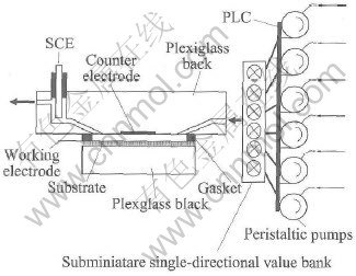
Fig.1 Schematic drawing of automated electrochemical thin-layer flow deposition reactor
Solutions were prepared with high purity reagents and twice-distilled water. All bismuth solutions consisted of 0.0001mol/L Bi(NO3)3・5H2O, and using 0.1mol/L HClO4 as a supporting electrolyte, pH 1.5. Tellurium solutions were all 0.0001mol/L in TeO2, and also used 0.1mol/L HClO4 as a supporting electrolyte. The pH 8.5 Te solutions were pH adjusted with ammonia. Various blank rinse solutions were also utilized, with a pH analogous to its respective deposition solution. All solutions were deaerated by blowing purified N2 gas through and over the solution for 30min. All experiments were performed at room temperature.
The XRD patterns were obtained with a Philips-PW 1710 X-ray diffractometer using CuKα radiation. SEM images were taken with a commercial instrument (Quanta 400). XPS spectra were obtained using AlKα (1486.6eV). The energy scale for XPS measurements was calibrated setting the Au 4f7/2 transition at a binding energy of 83.98eV.
3 RESULTS AND DISCUSSION
3.1 Tellurium electrochemical behavior
The voltammetry of Te on Pt in this solution are shown in Fig.2. There are two reductive voltammetric features; the first peak C1 occurs at about -0.2V (vs SCE). Integration of this peak corresponds to a Te coverage of approximately one-third of a ML, suggesting an apparently surface limited deposition of Te. ML in this case refers to an atomic layer of an element, not a compound ML, which is defined as being one adsorbate atom for each Pt surface atom. The reduction has been shown to be a four electrons process:
HTeO+2+3H++4e→Te+2H2O(1)
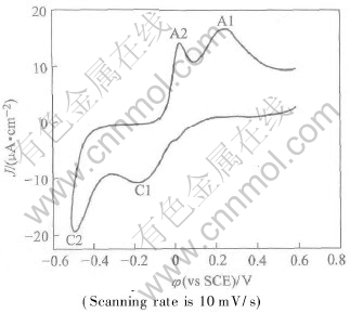
Fig.2 Cyclic voltammogram of 0.0001mol/L TeO2 in ammonia buffer solution of pH 8.5 on Pt
The second reduction feature C2 occurs near -0.5V and is the onset of bulk Te deposition. The subsequent anodic stripping peaks are also shown in Fig.1. The bulk stripping peak A2 is conjugated to the deposition peak C2, while A1 corresponds to stripping of the initial Te UPD peak, C1.
Studies by this group indicate that the Te UPD process is kinetically slow, even more as solutions become more basic, especially considering the scanning rate was only 10mV/s. This problem was circumvented by using what is referred to here as oxidative UPD. Due to the low concentration of HTeO+2 and the slow kinetics for Te deposition, very little Te(bulk) formed. The HTeO+2 solution was then exchanged for a blank electrolyte solution, and a potential sufficiently negative to reduce Te (bulk), but not negative enough to reduce Te (UPD), was applied:
Te(UPD)+Te(bulk)+H++2e→
Te(UPD)+HTe-(2)
Fig.3 shows CVA in the pH 8.5 blank solution containing no Te redox system. The reduction process at about -1.0V only involves bulk deposited Te. When the potential is scanned towards more negative values, the second reduce of Te underpotential peaks occurs giving an very narrow and sharp shape current peak.
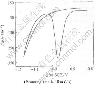
Fig.3 Cyclic voltammogram of bulk deposited Te reduction to Te2- in ammonia buffer solution of pH 8.5
3.2 Bismuth electrochemical behavior
Fig.4 shows the current-potential curves for different Bi concentration deposition and stripping on a Pt substrate. The relatively broad cathodic peak between 0.5V and 0V, labeled C1, and the stripping peak, labeled A1, are practically coincident, in spite of the concentration change. This suggested A1 and C1 to be conjugative deposition and stripping UPD peaks. In fact, because the UPD process is surface-limited, the charge involved in the UPD is independent of concentration: increasing concentration from 0.0001mol/L to 0.0004mol/L causes only the bulk redox process becomes more intensive. Fig.4 shows a clear difference between cathodic and anodic charge, which labeled C2 and A2 for the concentration variety, corresponding to the bulk reduction and oxidation respectively.
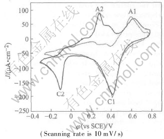
Fig.4 Cyclic voltammograms of Bi on Pt obtained from 0.0001mol/L (dot line) and
0.0004mol/L (solid line) Bi(NO3)3・5H2O in prochloric acid solution
3.3 Deposition of bismuth telluride thin films
In the first attempt, we tried to deposit Te directly. Thus an alternative way was adopted: Te layer was deposited at -0.1V, followed by rinsing with a blank. The Bi blank solution was then introduced. The Te and Bi solutions differed in pH by several units, so that rinsing with the Bi blank solution served to condition the cell and the tubing prior to the introduction of the Bi solution, avoiding incidental stripping of previous Te UPD layer in a higher pH. The Bi solution was then pumped in and held quiescent at 0.2V, while Bi UPD layer was deposited. This reductive Te UPD/ reductive Bi UPD cycle is shown in Fig.5(a). By this procedure, we deposited up to 100 layers of bismuth and tellurium. Fig.6 shows plots of the charges for Bi and Te stripping as a function of the number of deposition cycles. The plots are approximately linear, thus suggesting a layer-by-layer growth. The ratio of the slope of the two plots in Fig.6 gives an integrated charge ratio value of 1∶1 for bismuth and tellurium. As HTeO+2 reduction is a four elec tron process, Bi3+ reduction is only a three electron process, therefore the stoichiometric ratio of bismuth to tellurium is 4∶3, deviating from the traditional compound Bi2Te3. The slight Te scarcity may be due to the incomplete charge transfer in HTeO+2 reduction for Te direct deposition. XPS analysis suggested the presence of a tellurium oxide. Fig.7 shows the Te3d spectrum, with an elemental tellurium peak at 573.90eV, and a significant peak at 577.15eV, indicating the presence of a tellurium oxide species. Excluding a possible oxidation of the sample during the transfer to the spectrometer, we attributed the oxidized state of Te to the incomplete charge transfer in HTeO+2 reduction, as indicated by the chronocoulometric measurements already (Fig.6).
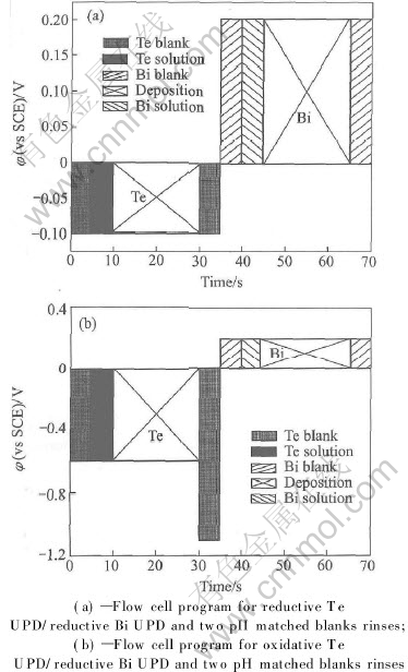
Fig.5 Diagram of an ECALE cycle for bismuth telluride formation
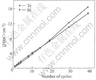
Fig.6 Plots of charge involved in oxidative stripping of Bi and Te as function of
number of ECALE cycles
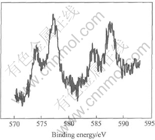
Fig.7 Te3d XPS spectrum for Te deposition at -0.1V on Bi deposited at 0.2V
In the second attempt, Te layers were deposited by reducing a small excess of bulk Te. We applied a potential equal to -0.6V for a deposition of bulk Te, and then a potential of -1.1V, which is sufficient to reduce bulk Te, but not the UPD Te. Bi layers were still deposited at 0.2V. The basic ECALE cycle for the deposition is schematized in Fig.5(b). The 200 alternative layers are deposited by this procedure. XPS quantitative analysis of the 200 cycles sample, obtained by this procedure, gave the 2∶3 stoichiometric ratio of Bi to Te, as expected for the formation of the Bi2Te3 compound.
Fig.8 shows XRD pattern of electrodeposited compound for 200 cycles. It can be seen that single phase Bi2Te3 compound is obtained except the prominent substrate [111] reflection. However, it reveals polycrystalline deposits. There are three primary reasons for the formation of polycrystalline deposits: the absence of an ordered substrate structure; lattice match between substrate and deposit; and substrate, solvent, reactant and electrolyte contamination. To address these problems and to promote the epitaxial electrodeposition of compound semiconductors, careful selection of lattice-matched single-crystal substrates will be necessary in order to avoid interfacial strain and promote ordered deposition.
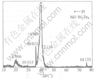
Fig.8 XRD pattern for 200-cycle Bi2Te3 deposit
Fig.9 shows the SEM image of a sample formed with 200 deposition cycles. The deposit looks like a series of buttons homogeneously distributed over the whole surface. The SEM micrograph shows distinct crystallites separated by grain boundaries and other crystallites without preferential orientation. This remark is confirmed by X-ray diffraction measurements obtained for films.
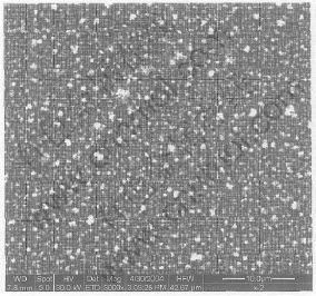
Fig.9 SEM image of sample formed with 200 deposition cycles of Bi2Te3 on Pt
One explanation for the morphology is that it results from the sequential preferential deposition of monolayers of Bi2Te3 on nucleation sites, on the surface. The buttons in Fig.9 are about 0.3-0.4μm in diameter. The crystal structure of bismuth telluride is rhombohedral with the space group (R3m). Crystal structure of Bi2Te3 along the XZ plane shows the quintuple layer leaves of Te-Bi-Te-Bi-Te separated by a Van der Waals gap. A monolayer of Bi2Te3 corresponds one fifteenth of the lattice constant for the hexagonal unit cell, 3.03nm or 0.202nm approximately. The expected thickness of the film would thus be 40.4nm for 200 cycles, or about 0.4μm, which is corresponding with the buttons diam. This suggests that the particle growth appears to be linear with the number of cycles, as it is consistent with a layer by layer growth mode.
The preferential nucleation sites mainly originate from the surface defects of the substrate by magnetic sputtering. In addition, the lattice mismatch of Pt with Bi2Te3 is close to 10%, which should result in the formation of an array of dislocations, within the first few deposited Bi2Te3 monolayers. It is clear that well-characterized single-crystal substrates should be employed and that top-quality morphology will be obtained much readily on an ordered, lattice-matched substrate.
4 CONCLUSIONS
The attempt to extend the ECALE methodology to the attainment of a typical Ⅴ-Ⅵ compound, such as Bi2Te3 on Pt, leads to a variation of the method since Te layers cannot be obtained by underpotential depositions directly. Thus, the reductive deposition of Te is combined with a bulk Te stripping to remove excess material. This process is referred to here as oxidative Te UPD. Oxidative UPD of Te and reductive UPD of Bi were alternated and repeated for 200 cycles. The resulting deposit was measured by XPS, XRD and SEM. The stoichiometric 2∶3 ratio of Bi∶Te, as expected for the formation of the compound, was confirmed by XPS analysis. XRD pattern shows a polycrystalline deposits. SEM image indicates that the diameter of deposit is consistent with calculated thickness of the epitaxial film. This suggests that the particle growth keeps to a layer by layer growth mode.
REFERENCES
[1]Venkatasubramanian R, Siivola E, Colpitts T, et al. Thin-film thermoelectric devices with high room-temperature figures of merit [J]. Nature, 2001, 413: 597-602.
[2]Das V D, Mallik R C. Study of scattering of charge carriers in thin films of (Bi0.25Sb0.75)2Te3 alloy with 2% excess Te [J]. Materials Research Bulletin, 2002, 37: 1961-1971.
[3]Zou H, Rowe D M, Williams S G. Peltier effect in a co-evaporated Sb2T3(P)-Bi2Te3(N) thin film thermocouple [J]. Thin Solid Films, 2002, 408: 270-274.
[4]Beyer H, Nurnus J, Bottner H, et al. High thermoelectric figure of merit ZT in PbTe and Bi2Te3-based superlattices by a reduction of the thermal conductivity [J]. Physica E, 2002, 13: 965-968.
[5]Aboulfarash B, Mzerd A, Giani A, et al. Growth of (BiSb)2Te3 thin films by metal-organic chemical varpour deposition [J]. Material Chemistry and Physics, 2000, 62: 179-182.
[6]Giani A, Boulouz A, Delannoy F P, et al. MOCVD growth of Bi2Te3 layers using diethyltellurium as a precursor [J]. Thin Solid Films, 1998, 315: 99-103.
[7]Miyazaki Y, Kajitani T. Preparation of Bi2Te3 films by electrodeposition [J]. J Crystal Growth, 2001, 229: 542-546.
[8]Golia S, Arora M, Sharma R K, et al. Electrochemically deposited bismuth telluride thin films [J]. Current Applied Physics, 2003, 3: 195-197.
[9]Flowers-Jr B H, Wade T L, Garvey J W, et al. Atomic layer epitaxy of CdTe using an automated electrochemical thin-layer flow deposition reactor [J]. J Electroanal Chem, 2002, 524-525: 273-285.
[10]Varazo K, Lay M D, Sorenson T A, et al. Formation of the first monolayers of CdTe on Au(111) by electrochemical atomic layer epitaxy (EC-ALE): studied by LEED, Auger, XPS, and in-situ STM [J]. J Electroanal Chem, 2002, 522: 104-114.
[11]Cecconi T, Atrei A, Bardi U, et al. X-ray photoelectron diffraction (XPD) study of the atomic structure of the ultrathin CdS phase deposited on Ag(111) by ECALE [J]. J Electron Spectroscopy and Related Phenomena, 2001, 114-116: 563-568.
[12]Innocenti M, Cattarin S, Cavallini M, et al. Characterisation of thin films of CdS deposited on Ag(111) by ECALE [J]. J Electroanal Chem, 2002, 532: 219-225.
[13]Pezzatini G, Caporali S, Innocenti M, et al. Formation of ZnSe on Ag(111) by electrochemical atomic layer epitaxy [J]. J Electroanal Chem, 1999, 475: 164-170.
[14]Innocenti M, Forni F, Pezzatini G, et al. Electrochemical behavior of As on silver single crystals and experimental conditions for InAs growth by ECALE [J]. J Electroanal Chem, 2001, 514: 75-82.
[15]Vaidyanathan R, Stickney J L, Cox S M, et al. Formation of In2Se3 thin films and nanostructures using electrochemical atomic layer epitaxy [J]. J Electroanal Chem, 2003, 559: 55-61.
[16]Vaidyanathan R, Stickney J L, Happek U, et al. Quantum confinement in PbSe thin films electrodeposited by elctrochemical atomic layer epitaxy [J]. Electrochimica Acta, 2004, 49: 1321-1326.
[17]Oznuluer T, Demir U. Formation of Bi2S3 thin films on Au(111) by electrochemical atomic layer epitaxy: kinetics of structural changes in the initial monolayers [J]. J Electroanal Chem, 2002, 529: 34-42.
[18]Zhou W P, Kibler L A, Kolb D M. Evidence for a change in valence state for tellurium adsorbed on a Pt(111) electrode [J]. Electrochimica Acta, 2002, 47: 4501-4510.
[19]Kuzume A, Herrero E, Feliu J M, et al. Copper underpotential deposition at high index single crystal surfaces of Au [J]. J Electroanal Chem, 2004, 570: 157-161.
[20]Kowalczyk P, Savard S, Lasia A. Determination of the adsorption energy distribution function of upd hydrogen on monocrystalline platinum [J]. J Electroanal Chem, 2004, 574: 41-47.
[21]Vracar L, Krstajic N, Neophytides S G, et al. Underpotential deposition of hydrogen on MoPt4 intermetallic phase in acid solution: temperature dependence [J]. International Journal of Hydrogen Energy, 2004, 29: 835-842.
Foundation item: Project(50401008) supported by the Chinese National Natural Science Foundation; Project(2004CCA03200) supported by the National Basic Research Program
Received date: 2004-11-22; Accepted date: 2005-01-18
Correspondence: YANG Jun-you, Professor; Fax: +86-27-87543776; E-mail: jyyang@public.wh.hb.cn
(Edited by HE Xue-feng)

