新型高速低功耗CMOS动态比较器的特性分析
吴笑峰1, 2,刘红侠1,石立春1,李 迪1,胡仕刚1
(1. 西安电子科技大学 微电子学院 宽禁带半导体材料与器件教育部重点实验室,陕西 西安,710071;
2. 湖南科技大学 信息与电气工程学院,湖南 湘潭,411201)
摘 要:为了降低sigma-delta模数转换器功耗,针对应用于sigma-delta模数转换器环境的UMC 0.18 μm工艺,提出1种由参考电压产生电路、预放大器、锁存器以及用作输出采样器的动态锁存器组成的新型高速低功耗的CMOS预放大锁存比较器。该比较器中输出采样器由传输门和2个反相器组成,可在较大程度上减少该比较器的功耗。电路采用标准UMC 0.18 μm工艺进行HSPICE模拟。研究结果表明:该比较器在1.8 V电源电压下,分辨率为8位,在40 MHz的工作频率下,功耗仅为24.4 μW,约为同类比较器功耗的1/3。
关键词:预放大锁存比较器;sigma-delta ADC;输出采样器;CMOS工艺
中图分类号:TN432 文献标识码:A 文章编号:1672-7207(2009)05-1354-06
Characteristic analysis of a new high-speed and low-power CMOS dynamic comparator
WU Xiao-feng1, 2, LIU Hong-xia1, SHI Li-chun1, LI Di1, HU Shi-gang1
(1. Key Laboratory for Wide Band-Gap Semiconductor Materials and Devices of Ministry of Education, School of Microelectronics, Xidian University, Xi’an 710071, China;
2. School of Information and Electrical Engineering, Hunan University of Science and Technology, Xiangtan 411201, China)
Abstract: To reduce power dissipation of a sigma-delta analog-to-digital converter, a new high-speed and low-power dissipation CMOS preamplifier-latch comparator, which is suitable for use in a sigma-delta analog-to-digital converter, was presented in CMOS 0.18 μm technology. The comparator consists of a reference voltage generation circuit, a preamplifier and a latch stage followed by a dynamic latch that operates as an output sampler. The output sampler circuit consists of a full transmission gate(TG) and two inverters. The use of this sampling stage results in the reduction in the power dissipation of the high-resolution comparator. Hspice simulations of the proposed circuit in a UMC 0.18 μm standard CMOS technology operating at supply voltage of 1.8 V was made. The results show that the resolution is 8 bit and the power dissipation is only 24.4 μW at 40 MHz. The power dissipation is about 1/3 of that of the similar comparators.
Key words: preamplifier-latch comparator ; sigma-delta ADC; output sampler; CMOS process
比较器是模拟集成电路设计中的1个基本模块,被广泛应用于模/数[1](A/D)和数/模(D/A)转换器中。在大多数情况下,比较器采用正反馈来提高结果的收敛速度。1种基本的比较器由2个反相器构成闩锁型,即1个反相器的输出端接另1个反相器的输入端而形成交叉耦合反相器[2-4]。在复位期间,闩锁比较器进入亚稳态。当复位结束时,比较器的闩锁节点被触发成2个稳态(电源电压或者零电压)中的1个,由此输出端输出相应的逻辑值[5-7]。传统比较器由几级(前置)放大器和锁存器组成[8-10]。在这种传统结构中,当处于再生过程时,最后一级锁存器中交叉连接的反相器构成正反馈,并在比较器的输出端产生轨对轨电压。在该过程中,通过2个交叉连接的反相器从电源电压VDD到地形成了1条低阻抗通路。因此,最后一级锁存级的功耗很大。本文作者提出的比较器的主要组成部分有:参考电压产生电路,预放大器和锁存器。该比较器通过使用输出采样器作为最后的锁存器来减少功耗,同时,维持高速性能。1个传输门(TG)和2个反相缓冲器用于实现输出采样电路。预放大器能提高放大器的分辨率,并能减少整个系统的失调。
1 比较器电路的结构分析与设计
在ADC中,通常在比较器前加1个前置放大器,这些前置放大器能提高放大器的分辨率,并且能减少整个系统的失调。但基于前置放大器的比较器其主要缺点是恒定静态功耗较高。而在A/D转换器中,总功耗中的大部分主要源于需要直流偏置电流的模拟电路部分所需要的静态功耗,1种有效的方法是使用动态比较器[11-13],这样,静态功耗就会减少。在A/D转换器中,为了满足分辨率、转换率、输入电压范围、功耗和面积等技术指标,需进行比较器设计。为研发高速、低功耗比较器,本文作者提出1种新颖的动态预放大-锁存比较器结构,其主电路如图1~3所示。主电路包括:参考电压产生电路、预放大器、锁存器。

图1 参考电压产生电路
Fig.1 Reference voltage generation circuit
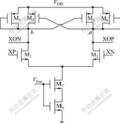
图2 预放大器电路
Fig.2 Preamplifier circuit
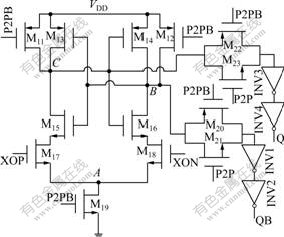
图3 锁存器结构
Fig.3 Latch architecture
图1所示为参考电压产生电路,这是1个典型的开关电容参考电压产生电路,可以根据电容的比值调节参考电压。其工作原理是:当P1为高电平时,VREF+给电容C充电,C上的电荷为(VREF-VCMI)?C。其中,时钟控制信号P1P的上升沿与P1的上升沿平齐,而其下降沿则在P1的下降沿之前,以实现底板采样,消除由于开关的电荷注入带来的非线性;当P2为高电平时,原来电容C在P1时充电的电荷在C和3C之间发生转移,根据电荷守恒,有:
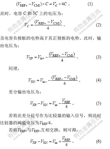
显然,此时比较器的阈值为-VREF/4。
如果图1中的所有电容均为C,则根据上面的分析可以得到比较器的阈值电压为VREF/2。同样,只要交换VREF+与VREF-的位置即可获得阈值电压-VREF/2。
图2所示为增益自举预放大器电路,图4所示为其小信号等效电路,其电压增益[14]的分析过程如下。
对图4中的a和b 2点列节点方程:
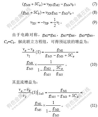
由于M3,M4,M5和M6都处于饱和态,其过驱电压相等,只要调整M3,M4,M5和M6的宽长比,便可调整gM3与gM5之比。例如,若gM3与gM5之比为3?4,则采用增益自举电路后,预运放的增益提升了4倍。

图4 预放大器的小信号等效电路
Fig.4 Preamplifier small signal equivalent circuit
图3中,M11~M19构成锁存器,M20和M21(M22和M23)构成1个传输门;INV1~INV4为4个反相缓冲器。1个完整的传输门(TG)和2个反相缓冲器组成输出采样电路[15],即M20和M21以及INV1和INV2为输出采样电路,M22和M23以及INV3和INV4为输出采样电路。CMOS 锁存器电路的组成为:2个NMOS差分输入对M17~M18,反相器M13~M15和M14~M16构成正反馈,M11~M12为预充电管,M19提供偏置电流。电容CA表示节点A的寄生电容,CL表示输出节点B和C的寄生电容。锁存器电路的动态工作分成复位阶段和再生阶段2个时间段。
a. 复位阶段。当P2PB信号电压较低时,比较器处于复位阶段。此时,M11~M12导通,M19截止,在电源电压和信号地之间没有电流回路,预充电MOS 管M11~M12将vB和vC拉到电源电压VDD,vB和vC被拉到电源电压VDD后,迫使M17和M18的漏极电压也接近于VDD。
b. 再生阶段。当P2PB信号电压较高时,比较器进入再生阶段。在再生阶段,M19导通,M11~M12截止,输出节点vC通过晶体管M15,M17和M19放电,输出节点vB通过晶体管M16,M21和M22放电。输出节点放电速度依赖于输入电压,如当vXOP>vXON时,vC放电快。假设M13和M14有相同的阈值电压,节点vC达到M14的阈值电压要比vB达到M13的阈值电压要早,由于正反馈,锁存结构M13,M14,M15,M16把vC拉至0,把vB拉至电源电压VDD。在此过程中,输出节点的放电时间与锁存器电路的再生时间之和的表达式为[15]:

2 结果分析与讨论
在UMC 混合/射频0.18 μm 1P6M P衬底双阱CMOS工艺条件下,对所提出的预运放-锁存比较器采用HSPICE仿真,仿真条件如下:时钟信号频率为40 MHz;电源电压为1.8 V;温度为125 ℃;工艺角模型为SS(slow NMOS+slow PMOS);预运放输入共模电压VCMI为 0.9 V;预运放尾电流源电流为15 μA;比较器输入差分电压为0.215 mV;比较器输出端电容负载为0.1 pF。
图5所示为控制比较器工作的各相时钟波形。图6所示为比较器在所有最坏输入条件下瞬态仿真波形。其中,v(P1)为节点P1(见图1)的电压,其余类推。可以看出,当差分输入电压从+(或-)1.8 V跳变到+ (或-)0.215 mV,或者从+(或-)0.215 mV跳变到+ (或-)1.8 V时,比较器都能输出正确的比较结果。这表明所提出的比较器在上述仿真条件下的差分输入范围为-1.8~1.8 V,能分辨的最小差分电压为0.215 mV。
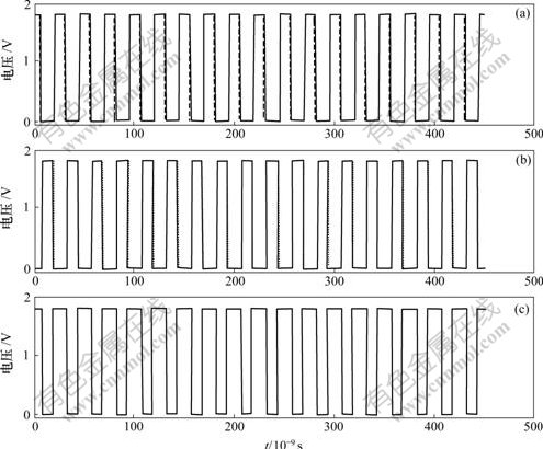
(a) v(P1)(实线), v(P1P)(虚线); (b) v(P2)(虚线), v(P2P)(实线); (c) v(P2PB)
图5 比较器工作的各相时钟波形
Fig.5 All clock waveforms of comparator

(a) v(P2)(实线), v(P2PB)(虚线); (b) v(VIN+-VIN-)(实线), v(XP)-v(XN)(虚线); (c) v(Q)
图6 比较器在各种最坏情况下的瞬态仿真结果
Fig.6 Simulated transient waveforms of comparator during all worst-case comparisons
图7所示为比较器的电源电流及其平均值。可以看出,供给比较器的电源电流在18个时钟周期内的平均值为13.546 μA,因此,比较器的功耗仅为24.4 μW。图8所示为经过HSPICE 100次Monte Carlo仿真后用MATLAB作出的比较器失调电压分布。经计算,失调电压的均值为2.04 mV,方差为20.64 μV,最大值为12 mV,最小值为-10 mV。因此,该比较器输入失调电压为22 mV。又由于所提出的比较器的输入范围为-1.8~1.8 V,所以,比较器在上述仿真条件下的分辨率达到8位。图9所示为一宽带低失真sigma-delta ADC中的4位flash ADC版图(该flash ADC包含16个所设计的比较器),该sigma-delta ADC中的调制器部分采用2-2级联前馈sigma-delta调制器,其第1级中的量化器为1位,第2级的量化器为4位。

(a) i(vtest-cmp); (b) v(P2)
图7 18个时钟周期时比较器的电源电流及其平均值
Fig.7 Supply current of comparator and its average value at 18 clock periods
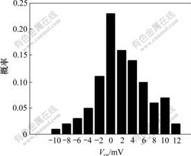
均值为2.04 mV;方差为20.64 μV
图8 比较器的失调电压分布
Fig.8 Histogram of comparator’s offset voltage
表1所示为比较器性能指标仿真比较结果。可以看出,本文设计的比较器在失调电压、工作频率以及功耗等方面均优于文献[11-13]中所设计的比较器。这种比较器低功耗、高速的特性使得其特别适合于多位宽带sigma-deltaADC如IEEE802.11b的应用中。如在sigma-deltaADC中使用N位量化器,所需比较器的个数为2N,那么,量化器的功耗随N呈幂级数增加,因此,低功耗比较器的使用具有极大的优势,因为它为sigma-deltaADC其余模拟电路模块的设计提供了更大的功耗设计余度。
表1 比较器性能指标仿真结果比较
Table 1 Summary of simulated comparator’s performance
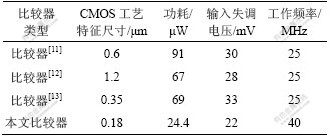
从表1可以看出,与传统的比较器相比,本文所提出的动态比较器精度为8位,输入失调电压为22 mV,最高工作频率为40 MHz,功耗仅为24.4 μW,约为同类比较器功耗的1/3。
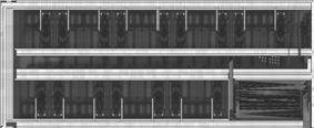
该flash ADC包含16个文中设计的比较器
图9 sigma-delta ADC中的4位flash ADC版图
Fig.9 Die photo of 4-bit flash ADC in sigma-delta ADC
3 结 论
a. 针对0.18 μm工艺应用于sigma-delta模数转换器环境,提出了由参考电压产生电路、预放大器、锁存器以及用作输出采样器的动态锁存器组成的新型高速低功耗CMOS预放大锁存比较器,与传统的比较器相比,该比较器无需前置放大器和输入失调抵消电路,从而在很大程度上降低了比较器的功耗。
b. 对所提出的比较器于单电源电压1.8 V环境中工作,采用UMC混合/射频0.18 μm1P6MP衬底双阱CMOS工艺对其进行设计实现,比较器精度为8位,输入失调电压为22 mV,最高工作频率为40 MHz,功耗仅为24.4 μW,约为同类比较器功耗的1/3。
参考文献:
[1] 凌玉华. 高速高精度模/数转换的微机动态轨道衡[J]. 中南工业大学学报: 自然科学版, 1999, 30(6): 623-625.
LING Yu-hua. A microcomputerizer dynamic railway scale with high-speed and high-glass accuracy A/D conversion[J]. Journal of Central South University of Technology: Natural Science, 1999, 30(6): 623-625.
[2] Veendrick H J M. The behavior of flip-flops used as synchronizers and prediction of their failure Rate[J]. IEEE J Solid-State Circuits, 1980, 15(2): 169-176.
[3] Boni A, Chiorboli G, Morandi C. Dynamic characterisation of high-speed latching comparators[J]. IEEElectron Lett, 2000, 36(5): 402-404.
[4] Sumanen L, Waltari M, Hakkarainen V, et al. CMOS dynamic comparators for pipeline A/D converters[J]. IEEE Int Symp on Circuit and Systems, 2002, 5: 157-160.
[5] Goll B, Zimmermann H. A low-power 2-Gsample/s comparator in 120 nm CMOS technology[C]// Proceedings of ESSCIRC. Grenoble, France, 2005: 507-511.
[6] Uyttenhove K, Steyaert M S J. A 1.8 V 6-Bit 1.3 GHz flash ADC in 0.25 m CMOS[J]. IEEE J Solid-State Circuits, 2003, 38(7): 1115-1122.
[7] Wong K L J, Yang C K K. Offset compensation in comparators with minimum input-referred supply noise[J]. IEEE J Solid-State Circuits, 2004, 39(5): 837-840.
[8] Abidi C. A 6b 1.3Gsample/s A/D converter in 0.35 μm CMOS[J]. IEEE J Solid-State Circuits, 2001, 36: 1847-1858.
[9] Dalton M. A 500-MSample/s, 6-b nyquist-rate ADC for disk drive read-channel application[J]. IEEE J Solid-State Circuits, 1999, 34: 912-920.
[10] Sheikhaei S, Mirabbasi S, Ivanov A. A 0.35 μm CMOS comparator circuit for high-speed ADC applications[C]//IEEE Int Symp Circ and Syst. 2005: 6134-6137.
[11] Abo A M, Gray P R. A 1.5-V, 10-bit,14.3-MS/s CMOS pipeline analog-to-digital converter[J]. IEEE J Solid-State circuits, 1999, 34(5): 599-606.
[12] Song W-Chul. A 10-b 20-Msample/s low-power CMOS ADC[J]. IEEE J Solid-State Circuits, 1995, 30(5): 514-521.
[13] Amaral P, Goes J. An improved low-voltage low-power CMOS comparator to be used in high-speed pipelined ADCs[C]//IEEE Int Symp Circ and Syst. 2002: 141-144.
[14] Razavi B. Design of analog CMOS integrated circuits[M]. New York: McGraw-Hill, 2001.
[15] Yin G M, Eynde F Opt, Sansen W. A High-Speed CMOS Comparator with 8-b Resolution[J]. IEEE J Solid-State Circuits, 1992, 27(2): 208-211.
收稿日期:2008-12-17;修回日期:2009-03-23
基金项目:国家自然科学基金资助项目(60206006);教育部新世纪优秀人才计划项目(NCET-05-0851);教育部科技创新工程重大项目培育资金资助项目(708083);西安应用材料创新基金资助项目(XA-AM-200701)
通信作者:吴笑峰(1974-),男,湖南涟源人,讲师,博士研究生,从事高速高精度模数转换器设计的研究;电话:15829738218;E-mail: willow_wxf@hotmail.com

