�Ƚ��ĵ��Ӷϲ�ɨ�輼���ڲ��Ͽ�ѧ�еķ�չ�������������������ɨ�����������
��Դ�ڿ����й���ɫ����ѧ��(Ӣ�İ�)2014���10��
�������ߣ���ï�� ������ �� �� �� �� �� ΰ �� �� ��̸�
����ҳ�룺3031 - 3050
Key words��electron tomography; materials science; transmission electron microscopy; scanning transmission electron microscopy
ժ Ҫ�������˻��������������ɨ������������ĵ��Ӷϲ�ɨ�輼���ڲ��Ͽ�ѧ��������½�չ����ϸ���������ֵ��Ӷϲ�ɨ������ͣ���������������Ķϲ�ɨ�輼�����������ϲ�ɨ�衢�����ϲ�ɨ�衢���������ϲ�ɨ�衢���ΰ����ϲ�ɨ����������˶ϲ�ɨ�裻����ɨ������������Ķϲ�ɨ�輼�������߽ǻ��ΰ����ϲ�ɨ�衢���ΰ����ϲ�ɨ�裬�ǹ��������ϲ�ɨ�衢����������ʧ�ϲ�ɨ���X�������ϲ�ɨ�衣�������Ż�����תϵ�У�����˫����ת��ͬ����ת������ת�Լ���б����ת�ȡ��ܽ����Ƚ����ع��㷨������ɢ�����ع�������ѹ�������㷨�Լ���б���㷨���������˵��Ӷϲ�ɨ�輼���ڲ��Ͽ�ѧ�еķ�չ���ơ�
Abstract: The recent developments of electron tomography (ET) based on transmission electron microscopy (TEM) and scanning transmission electron microscopy (STEM) in the field of materials science were introduced. The various types of ET based on TEM as well as STEM were described in detail, which included bright-field (BF)-TEM tomography, dark-field (DF)-TEM tomography, weak-beam dark-field (WBDF)-TEM tomography, annular dark-field (ADF)-TEM tomography, energy-filtered transmission electron microscopy (EFTEM) tomography, high-angle annular dark-field (HAADF)-STEM tomography, ADF-STEM tomography, incoherent bright field (IBF)-STEM tomography, electron energy loss spectroscopy (EELS)-STEM tomography and X-ray energy dispersive spectrometry (XEDS)-STEM tomography, and so on. The optimized tilt series such as dual-axis tilt tomography, on-axis tilt tomography, conical tilt tomography and equally-sloped tomography (EST) were reported. The advanced reconstruction algorithms, such as discrete algebraic reconstruction technique (DART), compressed sensing (CS) algorithm and EST were overviewed. At last, the development tendency of ET in materials science was presented.
Trans. Nonferrous Met. Soc. China 24(2014) 3031-3050
Mao-hua LI1, Yan-qing YANG1, Bin HUANG1, Xian LUO1, Wei ZHANG1, Ming HAN1, Ji-gang RU2
1. State Key Laboratory of Solidification Processing, Northwestern Polytechnical University, Xi��an 710072, China;
2. Beijing Institute of Aeronautical Materials, Beijing 100095, China
Received 24 November 2013; accepted 12 May 2014
Abstract: The recent developments of electron tomography (ET) based on transmission electron microscopy (TEM) and scanning transmission electron microscopy (STEM) in the field of materials science were introduced. The various types of ET based on TEM as well as STEM were described in detail, which included bright-field (BF)-TEM tomography, dark-field (DF)-TEM tomography, weak-beam dark-field (WBDF)-TEM tomography, annular dark-field (ADF)-TEM tomography, energy-filtered transmission electron microscopy (EFTEM) tomography, high-angle annular dark-field (HAADF)-STEM tomography, ADF-STEM tomography, incoherent bright field (IBF)-STEM tomography, electron energy loss spectroscopy (EELS)-STEM tomography and X-ray energy dispersive spectrometry (XEDS)-STEM tomography, and so on. The optimized tilt series such as dual-axis tilt tomography, on-axis tilt tomography, conical tilt tomography and equally-sloped tomography (EST) were reported. The advanced reconstruction algorithms, such as discrete algebraic reconstruction technique (DART), compressed sensing (CS) algorithm and EST were overviewed. At last, the development tendency of ET in materials science was presented.
Key words: electron tomography; materials science; transmission electron microscopy; scanning transmission electron microscopy
1 Introduction
TEM is an important tool that can provide valuable information about the microstructure and chemistry of materials at nanoscale. However, TEM images are only two-dimensional (2D) projections of three-dimensional (3D) objects, and therefore these images provide only partial information, even erroneous information in some case because of lack of depth resolution. To understand accurately the relationships between the structures and the properties, it is essential to view directly in 3D, especially for materials with complex morphology and chemistry.
More recently, electron tomography (ET) has been successfully applied to 3D reconstruction of nanostructures with the morphologies and chemical compositions. Although the mathematical base for tomographic techniques had been established in 1917 by RADON [1], it was firstly applied to ET in biological sciences in 1968 [2,3]. With the advent of the novel tomographic imaging modes, the automation of microscope control, the optimized tilt series and the advanced reconstruction algorithms, ET has acquired revolutionary development, and has been widely used in the field of materials science in the past several decades.
According to imaging modes of ET, the types of ET based on TEM and STEM include BF-TEM tomography [4-8], DF-TEM tomography [9], WBDF-TEM tomography [10-12], ADF-TEM tomography [13], EFTEM tomography [14-19], HAADF-STEM tomography [20-28], ADF-STEM tomography [29,30], IBF-STEM tomography [31], EELS-STEM tomography [32-34], XEDS-STEM tomography [35-37], and so on. Lately, ZEWAIL [38] and KWON and ZEWAIL [39] have pioneered four-dimensional (4D) ultrafast electron microscopy (UEM) with spatial and temporal resolution, which makes dynamics ET implement.
ET mainly consists of three steps: tomography data acquisition, tomography alignment and reconstruction, and tomography visualization. In order to be suitable for tomography, all image signals along the tilt series must strictly meet the projection requirement, namely the recorded signals must be a monotonic function of some physical properties of the object.
The aim of this review is mainly firstly to summarize the novel tomographic imaging modes, then to introduce the optimized tilt series and the advanced reconstruction algorithms, and finally to present the further developments of ET.
2 Novel tomographic imaging modes
2.1 Based on TEM
2.1.1 BF-TEM tomography
BF-TEM tomography is suitable for amorphous materials, where mass thickness contrast is dominant. A few successful examples were reported, such as studying the location and distribution of metal (oxide) particles in zeolites and catalyst materials in 3D, and the location and the connectivity of pores in mesoporous materials [4-8]. Figure 1 shows the 3D reconstruction of an Au/SBA-15 model catalyst particle, revealing the size and location of Au particles inside the support material clearly [8]. However, for crystalline materials, BF-TEM images are mainly dominated by diffraction contrast that is highly sensitive to the direction of the incident beam. Therefore, it is very difficult to obtain BF-TEM images with clear contrast through the entire tilt range. In general, BF-TEM tomography is unsuitable for crystalline materials.
2.1.2 DF-TEM tomography
In general, DF-TEM images do not fulfill the projection requirement because the image intensity varies rapidly in a complicated manner with sample orientation. It is very difficult to acquire a tilt series of DF-TEM images of a crystalline specimen for tomography. Fortunately, KIMURA et al [9] have successfully reconstructed the D1a-ordered Ni4Mo precipitates in Ni�CMo alloy by DF-TEM tomography, and introduced how to obtain a tilt series of DF-TEM images of the Ni4Mo precipitates. Firstly, a systematic row containing the D1a superlattice reflection at (4/5, 2/5, 0) was parallel to the tilt axis of the holder by placing carefully the specimen on the specimen holder, which made the D1a superlattice reflection exist in the tilt series from -60�� to +60�� (see Fig. 2(a)). Secondly, by adopting the (4/5, 2/5, 0) superlattice reflection, a tilt series of DF-TEM images of the Ni4Mo precipitates were recorded (see Fig. 2(b)). Finally, the 3D shape and position of the Ni4Mo precipitates were reconstructed (see Fig. 2(c)).
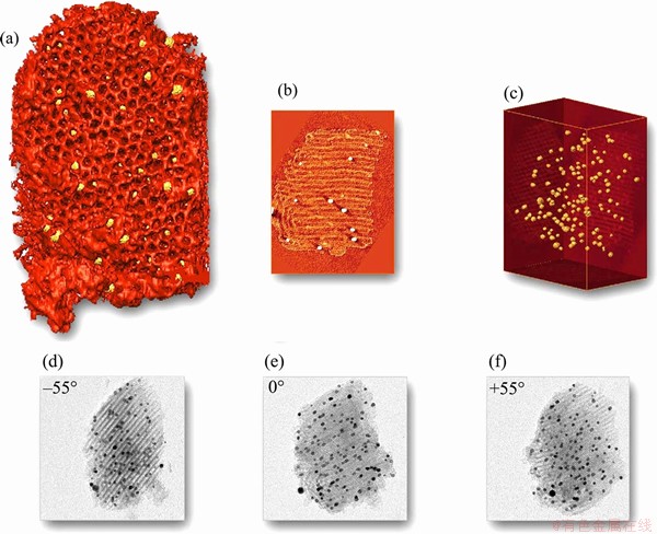
Fig. 1 Au catalyst nanoparticles inside SBA-15 mesoporous support (a), surface rendering of slice (b) from (a), surface rendering of Au nanoparticles only (c), BF images at -55�� (d), 0�� (e) and +55�� (f) [8]
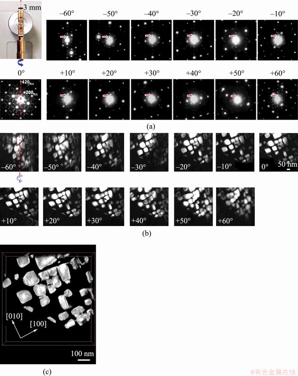
Fig. 2 Specimen holder and part of electron diffraction patterns along tilt series in Ni-18%Mo (mole fraction) alloy (All red arrows indicate a D1a superlattice reflection at (4/5, 2/5, 0) (a), DF images of D1a-ordered Ni4Mo precipitates at different tilt angles (b) and 3D reconstruction (c) of Ni4Mo precipitates from tilt series in (b) [9]
2.1.3 WBDF-TEM tomography
Although coherent diffraction contrast seems to violate the projection requirement, WBDF-TEM tomography has recently been proposed to investigate the 3D distribution of dislocation network in GaN film [10,11] and dislocation-precipitate interactions in an Al-Mg-Sc alloy [12]. Figure 3(a) shows the complex 3D dislocation network in a GaN epilayer, revealing threading dislocations at small-angle grain boundaries of individual domains (D), a dislocation bundle associated with a crack tip (B), in-plane dislocations caused by threading dislocations turning over (T), a jog of an in-plane dislocation by a threading dislocation (J), and mixed dislocation (M) [10]. Figures 3(b) and (c) show 3D relationships between the dislocations and the Al3Sc particle, among the twist boundary, the dislocations, and the Al3Sc particle, respectively. The WBDF-TEM technique is suitable for observation of dislocations because a WBDF-TEM image of dislocation is narrow in width and close to the dislocation core. Therefore, WBDF-TEM tomography is probable for 3D dislocation reconstruction. To meet the projection requirement, the WBDF-TEM condition must maintain constant through the entire tilt range, so that the dislocations are visible in the entire tilt series. Unfortunately, data acquisition in WBDF-TEM tomography is very difficult because the diffraction condition must be lined up exactly along the entire tilt range. Besides, during tilting, general acquisition software cannot automatically complete due to the unstable image contrast. Consequently, the tilt series of WBDF-TEM images have to be obtained manually.
2.1.4 ADF-TEM tomography
A schematic diagram of ADF-TEM is shown in Fig. 4(a). An annular objective aperture is inserted in the back focal plane of the objective lens, which shuts a central beam out [13,40-42]. As a consequence, ADF-TEM imaging only makes use of electrons that are scattered in 20-40 mrad. These electrons are dominated by phonon scattering [40]. Recently, BALS et al [13] have successfully applied ADF-TEM to the 3D reconstruction of CdTe tetrapods and C nanotubes filled with Cu nanoparticles. Figure 4(b) shows an ADF-TEM image of two CdTe tetrapods with CdSe (indicated by white arrows). Obviously, a distinction between CdSe (average Z=50) and CdTe (average Z=41) is possible. Figure 4(c) shows 3D CdTe tetrapods with the lighter CdSe part (indicated by a black arrow). The advantages of ADF-TEM can be summarized as follows: 1) generating a mass-thickness contrast that fulfills the projection requirement [41]; 2) generating an atomic number contrast, namely providing chemical information in TEM mode [13,42]; 3) shortening exposure time (only 1-3 s), which provides advantages of reducing beam damage to samples and avoiding scanning noise.
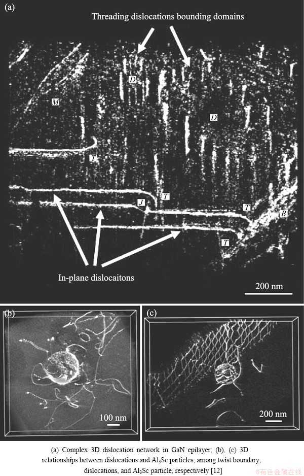
Fig. 3 3D reconstructions based on WBDF-TEM imaging
2.1.5 EFTEM tomography
EFTEM is able to map quantitatively the elemental species with a resolution of about 1 nm. Image signal is a monotonic function of elemental concentration and the projected specimen thickness, meeting the projection requirement. Moreover, EFTEM can strongly reduce diffraction effects. Thus, EFTEM tomography is suitable for reconstruction of 3D chemical maps on nanoscale. EFTEM tomography makes use of elemental maps or jump ratio maps as projections. In the past years, EFTEM tomography has been already used to investigate Y2O3 particles in polycrystalline FeAl [14,15], Cr carbides in 316 stainless steel [16], a chain of magnetite (Fe3O4) magnetosome in a magnetotactic bacteria (see Fig. 5(a)) [16], a C nanohorn with a Cu core (see Fig. 5(b)) [17], FeNi nanoparticles [18], N-doped carbon nanotubes [19], and so on. However, there are also some shortcomings in EFTEM ET: 1) only thin samples can fulfill the projection requirement, 2) signal-to-noise ratios are poor, and 3) the time of data acquisition is long in entire tilt series, making it unsuitable for beam-sensitive samples.
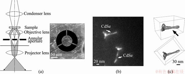
Fig. 4 Schematic diagram of ADF-TEM (left) and secondary electron image of annular aperture (right) (a), ADF-TEM image of two CdTe tetrapods (b) and isosurface visualization of 3D CdTe tetrapods by ADF-TEM tomography (c)
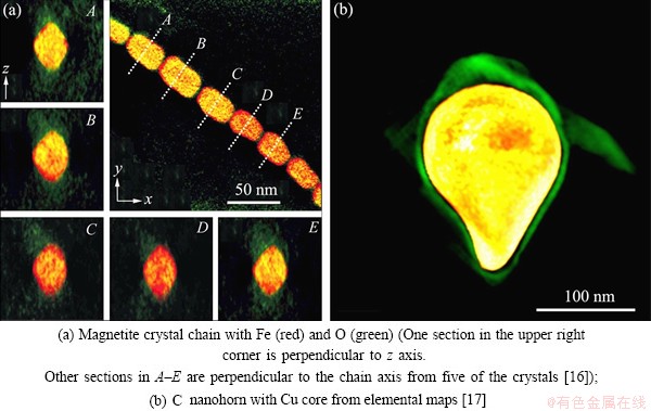
Fig. 5 EFTEM tomographic reconstructions
2.2 Based on STEM
2.2.1 HAADF-STEM tomography
HAADF-STEM makes use of an annular detector with a high inner collection angle (>60 mrad). Due to Rutherford elastic scattering, HAADF-STEM image intensity is typically dominated by atomic number (Zn (1.5
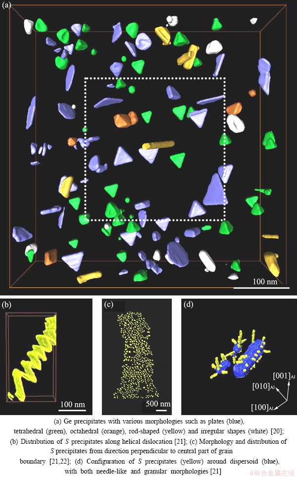
Fig. 6 3D reconstructions using STEM-HAADF tomography
Although HAADF-STEM tomography is a very powerful tool to reconstruct actual 3D structure of nanoscale materials with complex morphology and chemistry, it also has some unavoidable disadvantages. Exposure (scanning) time per image generally requires 10-30 s. Long time scanning not only produces more scanning noise but also makes it unsuitable for beam-sensitive samples. HAADF-STEM tomography is unfit for some nanostructures such as lattice defects, grain boundaries, orientation variants of ordered domains, because these nanostructures are only related to diffraction contrast images. HAADF-STEM tomography is unsuitable for multiphase materials which consist of the elements with neighboring atomic number because of low-contrast.
2.2.2 ADF-STEM tomography
Both the inner collection angle of an annular detector and the convergence angle for ADF-STEM imaging are smaller than that for HAADF-STEM imaging. TANAKA et al [29,30] have successfully reconstructed dislocations in a Si crystal by ADF-STEM tomography. Figure 7(a) shows a schematic diagram showing the diffraction vector of g=220 maintained in the annular detector during the entire tilt series. Figure 7(b) shows 3D dislocations viewed from different orientations. The dislocations are colored according to their slip systems.
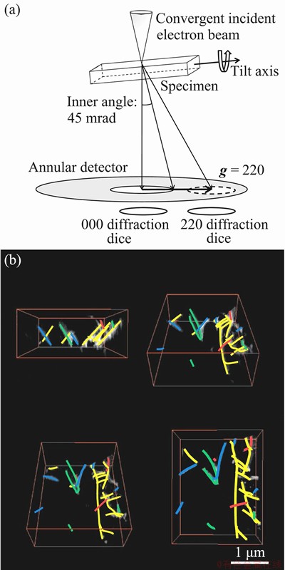
Fig. 7 Schematic diagram of diffraction vector of g=220 maintained in annular detector [29] (a), 3D reconstruction of dislocations in Si crystal by tilt series of ADF-STEM images (b) [30]
For dislocation, ADF-STEM tomography technique is more feasible than WBDF-TEM tomography. The reasons include the following aspects: 1) The ADF-STEM technique suppresses diffraction contrast because of multiple beams and the convergent beam, while the WBDF imaging utilizes only one reflection; 2) The ADF-STEM tomography allows large deviations from the exact diffraction vector to image dislocations along a tilt series, and the dislocation contrast is much more consistent by ADF-STEM imaging than by WBDF imaging in the entire tilt range. As a result, automation of data acquisition in ADF-STEM tomography is practicable for reconstruction.
2.2.3 IBF-STEM tomography
For HAADF-STEM technique, the acceptable sample thickness is 50-100 nm. When samples are thicker, the image contrast reversal would arise [31]. The reason for this phenomenon is that the thick and/or high atomic number materials lead to increased backscatter and multiple scattering events to high angles. The angle of the electron beam detector in IBF-STEM is generally set to be 0-100 mrad to suppress diffraction contrast, and avoid contrast reversal at all thick materials. ERCIUS et al [31] have investigated thick copper microelectronic structures with a stress void by IBF-STEM tomography and HAADF-STEM tomography, respectively (see Fig. 8). The results indicate that the 3D reconstruction using IBF-STEM imaging shows the precise location of the stress void without artifacts.
2.2.4 EELS-STEM tomography
EELS-STEM spectrum imaging is successfully utilized to analyze the elemental, physical and chemical state information in nanoscale materials [44-46]. In Refs. [32-34], researchers have used EELS-STEM tomography to probe a W-to-Si contact from semiconductor device, a ZnO thin film, mesoporous a Co3O4 particles filled with FexCo3-xO4 and multiwalled carbon nanotubes (MWCNT)�Cnylon nanocomposite in 3D. Figure 9(a) shows a schematic diagram revealing the collection of an energy-loss series at each tilt angle and each energy window with a specific voxel P in the 3D volume. Figure 9(b) shows surface renders of the MWCNT (purple) within the nylon (gray) viewed from different angles using plasmon-loss electrons. The hole in the nylon and the voids in the MWCNT are obviously visible in 3D [34].
2.2.5 XEDS-STEM tomography
Recently, XEDS spectrum imaging technique has been utilized to resolve 3D chemical studies in nanoscale materials [35-37]. Compared with HAADF-STEM tomography, XEDS-STEM tomography has obvious superiority in enhancing chemical contrast especially between neighboring atomic numbers in the multiphase materials. Compared with EFTEM and EELS spectrum imaging, XEDS imaging can obtain the maps of a large number of elements simultaneously. GENC et al [35] have demonstrated 3D distribution of elements in a Li1.2Ni0.2Mn0.6O2 (LNMO) nanoparticle based on XEDS-STEM imaging. Figure 10(a) shows 3D elemental distribution of Mn (red) indicating relatively homogeneous distribution of Mn in the nanoparticle. Figure 10(b) shows 3D elemental distributions of Ni (green) indicating segregation of Ni at grain boundaries and at some surface locations on the outer rim of the nanoparticle. Figure 10(c) shows 3D elemental distributions of Mn and Ni. Figure 10(d) shows 3D elemental distribution of O (blue) indicating fairly homogeneous distribution of O element in the nanoparticle. Figure 10(e) shows 3D elemental distributions of Mn and O.
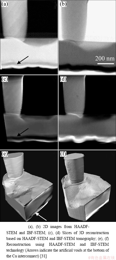
Fig. 8 Imaging stress void in copper interconnect with Ta electromigration liners
However, the geometry of traditional single detector limits acquisition of the XEDS imaging in a complete tilt series because the sample or the holder will shadow the single detector and the intensity of X-ray will vary significantly with the tilt angle of sample. This problem is able to be avoided using a needle specimen prepared by a focused-ion beam (FIB) instrument [36] or a symmetrically arranged four XEDS detectors [35], as shown in Fig. 11.
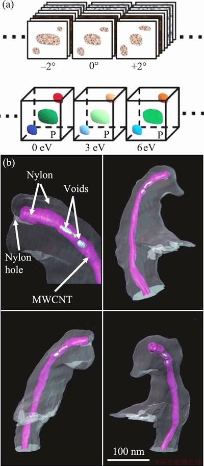
Fig. 9 Energy-loss series of 2D images at each angle and each energy window showing specific voxel P in 3D volume (a) and surface renders of MWCNT (purple) and nylon (gray) viewed from different angles (b) [34]
2.3 4D tomography
2.3.1 4D chemical composition
A spectroscopic electron microscopy makes use of inelastically scattered electrons, which can obtain mappings of elemental species over wide fields of view at nanoscale materials. The type of spectroscopic electron microscopy includes EFTEM [14-19], EELS-STEM [32-34] and XEDS-STEM [35-37]. The technique acquires a 4D data set I=I(x, y, ��, ��E), containing two spatial dimensions x and y, the rotation angle ��, and the selected spectrometer energy ��E.
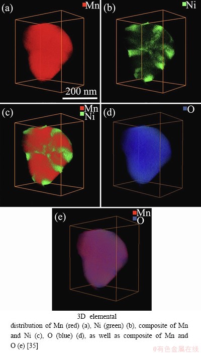
Fig. 10 Volume renders of 3D visualizations of LNMO nanoparticle using XEDS spectrum imaging
2.3.2 4D time
In order to better understand the relationship between the structures and the properties, dynamic ET is needed to study the nonequilibrium structures and complex transient processes. ZEWAIL [38] and KWON et al [39] have reported 4D UEM which possesses nanometer spatial resolution and femtosecond temporal resolution. The UEM records the images with ultrafast electron packets derived from a train of ultrafast (femtosecond or picosecond) pulses. KWON and ZEWAIL [39] have demonstrated the different motion modes of the carbon nanotubes with a bracelet-like ring structure using 4D UEM. Figure 12(a) shows a schematic diagram of 4D ET with time resolution. At t0, the heating pulse initiates the structural change. At t��, the time-delayed electron packet images the structure at a given tilt angle ��. Figure 12(b) shows a series of 2D images at various projection angles and time steps. Figure 12(c) shows 4D visualization of the nanotubes for two angles at relatively early time. The original volumes at t=0 and those volumes at different time delay are colored respectively by black and beige. Figure 12(d) shows 4D tomography of the bracelet at longer time. Different colors denote the volumes at different time delay. White arrows indicate the direction of breathing motion (see Fig. 12(c)) and wiggling motion (see Fig. 12(d)).
3 Optimized tilt series
During the process of acquiring the 2D projections, a tilt range of ��90�� is mostly improbable. The reasons are summarized as three respects: 1) The space between the specimen holder and the objective lens pole pieces is limited. For this reason, the tilting range of an advanced single-tilt tomography holder is at most ��80��; 2) The thickness of conventional TEM samples will dramatically increase with the increasement of the tilt angle. For example, the specimen thickness becomes twice at 60�� and close to three times at 70��; 3) The shadow arises due to the holder, grid or other parts of the specimen. The limited tilt range leads to a ��missing wedge�� of information (see Fig. 13(a)), which results in reconstruction artifacts such as fanning and elongation effects in the direction of the missing wedge, especially when the object is highly anisotropic [47,48].
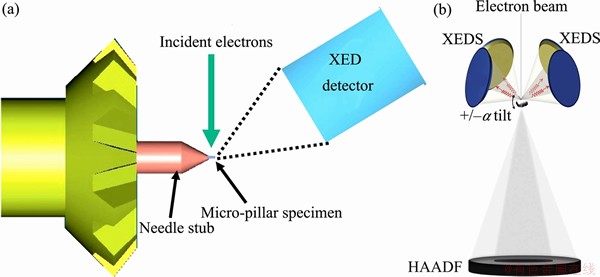
Fig. 11 Schematic diagrams of geometrical configuration between pillar-shaped specimen and XEDS detector [36] (a), and symmetrically arranged four XEDS detectors around specimen (b) [35]
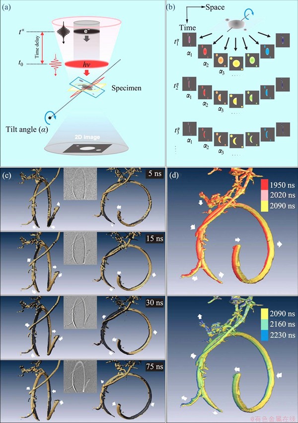
Fig. 12 Schematic diagram of 4D ET with time resolution (a), a series of 2D images at various projection angles and time steps (b), snapshots of 4D visualization of nanotubes for two angles at relatively early time (c) and 4D tomography of bracelet at longer time (d) (White arrows indicate the direction of motion) [39]
In order to reduce the missing wedge, several alternative techniques have been put forward, including dual-axis tilt tomography [47-50], on-axis tilt tomography [36, 51-53], conical tilt tomography [54], EST [55-57], and so on. This part will introduce the first three of these mentioned tilt series, EST will be highlighted in the next section of advanced reconstruction algorithms.
3.1 Dual-axis tilt tomography
For the so call ��dual-axis�� tilt series, 2D projections are acquired from two orthogonal single-axis tilt series [47-50], in which the second tilt series can be accomplished with rotating specimen by 90��. Using dual-axis tilt tomography, the missing wedge in Fourier space will be reduced to a missing pyramid (see Fig. 13(b)). Therefore, the dual-axis tilt technique can improve the fidelity of tomographic reconstructions and reduce artifacts. Figure 14 describes the 3D reconstructions of CdTe tetrapods from one single-axis tilt series, another perpendicular single-axis tilt series and dual-axis tilt series, respectively, showing the increase in the information of 3D reconstruction by dual-axis tilt series [47]. Figure 14(a) shows that some of the legs of the tetrapods are missing or weak due to the missing wedge (indicated by the arrows). In Fig. 14(b), although the missing legs in Fig. 14(a) are present, some legs from another direction are missing (indicated by the arrows). Figure 14(c) illustrates that no legs are missing. Figure 14(d) shows the magnification of the tetrapod boxed shown in Fig. 14(c).
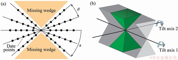
Fig. 13 Schematic diagram of missing wedge generated due to restricted tilt range in Fourier space (a) (�� is the sampling angle and �� is the maximum tilt angle) and missing wedge (gray) reduced to missing pyramid (green) by dual-axis tilt tomography (b) [47,48]
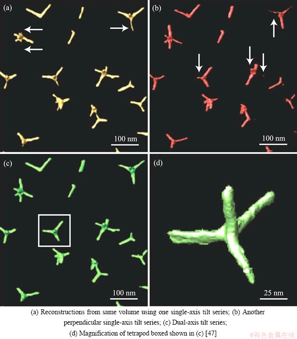
Fig. 14 3D reconstructions of CdTe tetrapods
3.2 On-axis tilt tomography
On-axis tilt is a full 360�� single-axis tilt. A micropillar sample mounted on a dedicated tomography holder is used in this technique, as shown in Fig. 11(a) [36,51-53]. It allows the sample to rotate over a tilt range of 360��. The size of specimens manufactured by a FIB technique is approximately 100-300 nm. The on-axis rotation holder is able to eliminate the missing wedge, thus, the fanning and elongation effects will be minimized [36,51-53]. KE et al [53] have demonstrated slices of the 3D reconstruction from carbon nanotubes (CNTs) inside semiconductor contact holes using two different tilt series: ��90�� (Figs. 15(a), (c)) and ��70�� (Figs. 15(b), (d)). Long white arrows indicate fanning effects due to the missing wedge in Figs. 15(b) and (d). A CNT (indicated by short white arrow) is clearly observed in Fig. 15(a), but is faint in Fig. 15(b). Another short white arrow (Fig. 15(d)) indicates a fanning effect, which might be misinterpreted as a CNT. The results indicate that on-axis tilt series can improve the fidelity of reconstructions. In addition, pillar-shaped specimens can be used to resolve the problem of the sample thickness increasing at higher tilt angles.
3.3 Conical tilt tomography
LANZAVECCHIA et al [54] have reported a conical tilt tomography. Through this method, the missing wedge in Fourier space will be reduced to the missing cone. Figure 16 shows the schematic diagrams of a single-axis tilt tomography, a dual-axis tilt tomography and a conical tilt tomography in Fourier space, from which it can be seen that the conical tilt tomography has smaller missing space. A conical tilt series is achieved by tilting the specimen to the maximum angle, and then rotating in small increments until completing a 360�� turn. The technique solves partly the missing wedge effect, especially for the samples with high anisotropy. However, the drawbacks of a conical tilt tomography are also present, such as increasing the number of projections, only partly eliminating the missing information and requiring a more elaborate specimen stage.
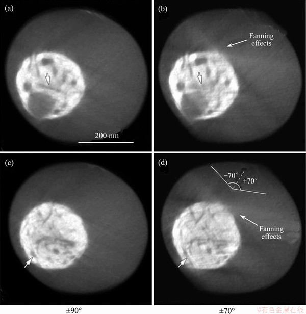
Fig. 15 Slices of CNTs grown inside semiconductor contact holes at two different positions using full ��90�� tilt series (a) and (c), and ��70�� tilt series (b) and (d), respectively) [53]
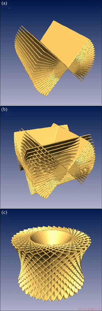
Fig. 16 Schematic diagram of single-axis tilt tomography with missing wedge in Fourier space (a), dual-axis tilt tomography with missing pyramid (b), and conical tilt tomography with missing cone (c) [54]
4 Advanced reconstruction algorithms
At present, for reconstruction, the widely used algorithms are weighted back-projection (WBP) algorithm and simultaneous iterative reconstruction technique (SIRT). Unfortunately, using the above two algorithms, the quality of reconstructions is poor because of reconstruction artifacts, such as streaking, fan or star artifacts, blurring and elongation. To reduce reconstruction artifacts resulting from the missing wedge and a limited number of projections, some advanced reconstruction algorithms with higher fidelity of reconstruction are adopted. The following mainly introduces three advanced reconstruction algorithms: DART [58-61], CS-ET [62-64] and EST [55-57].
4.1 DART algorithm
DART can be used to obtain high quality reconstructions in ET when the samples satisfy discrete constraints [58-61]. The so-called ��discrete constraints�� state that the samples consist of fewer compositions and each is corresponding to a unique grey level in reconstruction. The algorithm starts with a SIRT reconstruction and imposes the set of possible gray levels as additional reconstruction parameter. BIERMANS et al [58] have demonstrated the 3D reconstruction of a porous layer of La2Zr2O7 based on SIRT and DART from tilt series with missing wedges of 0��, 20��, 40�� and 60�� (see Fig. 17). Experimental results based on DART indicate that the missing wedge artifacts, such as elongation and fanning effects, are drastically reduced, and the effect of the missing wedge is less obvious.
DART has several major advantages. Firstly, missing wedge artifacts can be reduced significantly, correspondingly, reconstruction quality can be improved dramatically. Secondly, the number of required projection images can be reduced substantially, which makes it suitable for reconstructing beam-sensitive samples. Thirdly, quantitative information can be obtained automatically during the reconstruction. Finally, defect structures, such as vacancies, can be reconstructed by DART.
4.2 CS-ET
Recently, CS-ET has been introduced successfully to reconstruct 3D nanoscale structures [62-64]. The new reconstruction algorithm based on CS can be used to get a sparse solution or a solution with a sparse gradient during image processing. LEARY et al [63] have demonstrated 3D reconstructions of unsupported Ga-Pd nanoparticles based on CS-ET and SIRT, respectively (Fig. 18). Experimental results indicate that the missing wedge artifacts can be significantly reduced, and the nanoparticle boundaries are quite clear in the CS-ET reconstruction. Moreover, some smaller nanoparticles which are difficultly distinguished in the SIRT reconstruction can be obviously distinguished in the CS-ET reconstruction, as indicated by orange arrows.
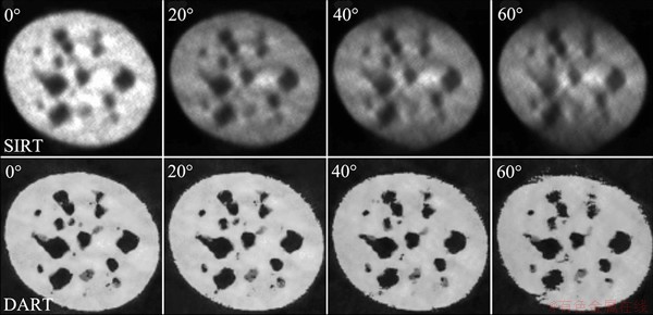
Fig. 17 Orthoslices through 3D reconstruction of porous layer of La2Zr2O7 based on SIRT (top), and DART (bottom) from tilt series with missing wedge of 0��, 20��, 40��, and 60�� [58]
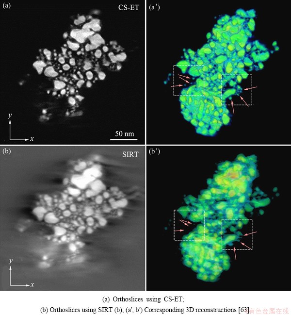
Fig. 18 3D reconstructions of unsupported Ga�CPd nanoparticles by HAADF-STEM tomography
CS-ET has several outstanding advantages: compensating for the missing wedge, being segmented easily and requiring fewer projections. As a result, the high fidelity of 3D reconstruction can be obtained based on CS-ET.
4.3 EST
EST acquires a tilt series of 2D projections with equal slope increments [55-57]. The technique makes use of pseudopolar fast Fourier transform and the oversampling method with an iterative algorithm. LEE et al [56] have demonstrated 3D reconstruction of single keyhole limpet hemocyanin (KLH) particles by EST for the first time. Figure 19(a) shows iso-surface renderings in different orientations of the model. Figures 19(b)-(g) show 3D reconstruction of KLH particles based on WBP-full, WBP-full-denoising, EST-full, WBP-2/3, WBP-2/3-denoising and EST-2/3, respectively. The WBP reconstructions have a few holes in this region (green arrows) in Figs. 19(c) and (f), but the EST reconstructions are more continuous and smoother in Figs. 19(d) and (g). Experimental results indicate that the reconstruction by EST has less noise, clear boundaries and continuous density. In general, there are some advantages in EST. Firstly, the EST method can alleviate the missing wedge artifacts. Secondly, it is suitable for beam-sensitive samples since a limited number of projections are enough to acquire precise reconstruction.
5 Ongoing research and future perspectives
5.1 New technique assisted ET
A novel technology of electron beam precession is able to reduce multiple scattering effects by rocking the beam around the optical axis [65,66]. REBLED et al [67] have carried out successfully 3D reconstruction of Sn precipitates embedded in Al matrix based on beam precession assisted ET, as shown in Fig. 20, in which the left column is without beam precession and the right column is with beam precession. Obviously, the images in right column present more homogenous background and more strong contrast features of the precipitate than those in left column. Especially, in Fig. 20(c), the precipitate is invisible due to the combination of the precipitate inherent diffraction contrast condition and the presence of thickness and bending artifacts, whereas in Fig. 20(c��) the precipitate is clearly visible. These results indicate that the combination of beam precession and BF-TEM can eliminate kinetic effect caused by multiple scattering, artifacts of thickness and bending. Therefore, high quality reconstruction can be obtained by this technique.
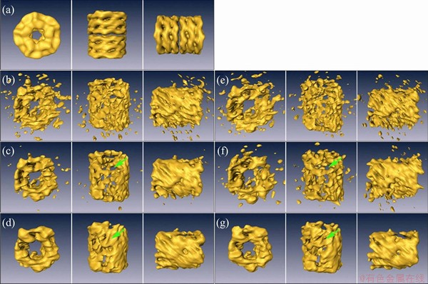
Fig. 19 Iso-surfaces of known higher resolution model viewed from different directions (a), 3D reconstructions of based on WBP-full (b), WBP-full-denoising (c), EST-full (d), WBP-2/3 (e), WBP-2/3-denoising (f) and EST-2/3 (g) (2/3 denotes reduced-dose reconstructions) [56]
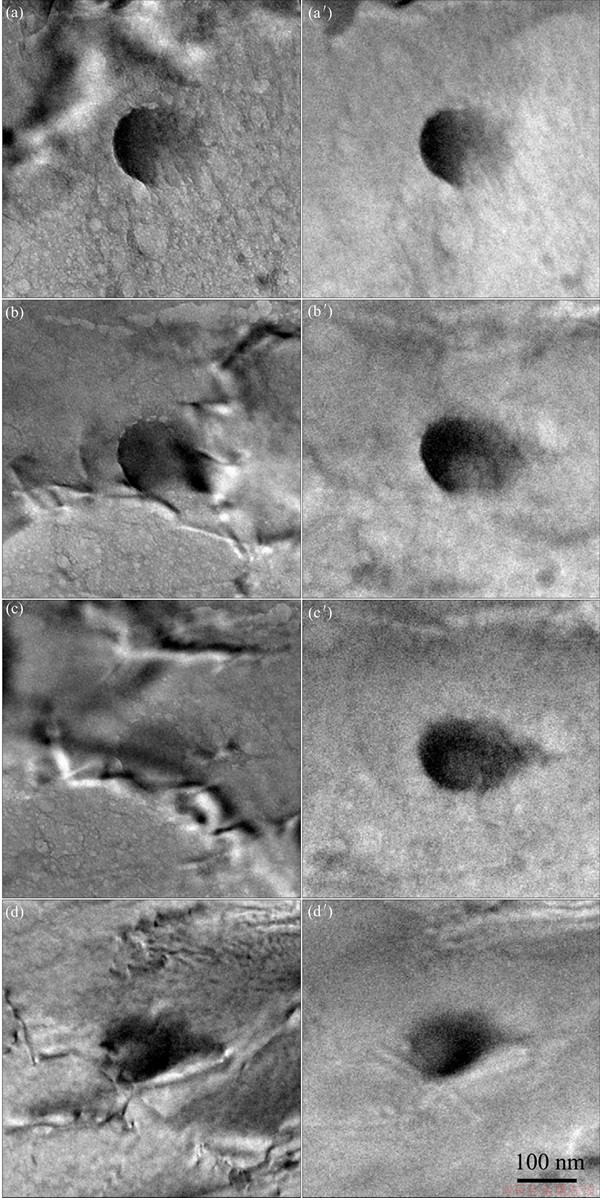
Fig. 20 BF-TEM images of Sn precipitate at 35�� (a, a��), +9�� (b, b��), -9�� (c, c��) and -43�� (d, d��) tilt angle [67]
5.2 Multi-signal and multi-dimensional electron tomography
Transmission electron microscope can generate various signals such as elastically scattered electrons, inelastically scattered electrons, and X-ray. ET can reconstruct materials at nanoscale by utilizing mass thickness maps [4-8], diffraction maps [9-13], elemental maps [13-28,32-37], thickness maps [17] and bulk plasmon maps [17], etc. With the development of the elemental mapping techniques in TEM, STEM and UEM, ET can obtain 4D reconstruction through space-energy maps [14-19, 32-37], energy-time maps [68-70] and space-time maps [38,39].
5.3 High resolution electron tomography
In general, the resolution of ET is limited to the nanometer range. The resolution is affected by several factors, such as the resolution of electron microscope, the alignment of the projections, the number of projections, the missing wedge and the thickness of the sample. However, the ultimate goal of ET is the acquisition of atomic-resolution in 3D. In recent few years, researchers [57,71-77] have successfully demonstrated 3D reconstruction at atomic resolution by different techniques, such as the combination of aberration- corrected electron microscopy and advanced reconstruction algorithm (such as DART, CS-ET and EST) [57,71-76], ��Big Bang�� tomography based on focal series reconstruction or off-axis holography [77]. Figure 21 shows two examples of atomic-resolution 3D reconstruction, showing 3D structure of the Au nanoparticles at the two-fold (see Fig. 21(a)) and two selected slices of volume rendering of Au nanorods (see Fig. 21(b)) [57,71].
6 Conclusions
ET is a promising technology that can obtain the 3D information of the morphologies and chemical compositions of nanostructures. In the last few decades, ET has acquired revolutionary development. The recent developments of ET depend upon the novel tomographic imaging modes, the automation of microscope control, the optimized tilt series and the advanced reconstruction algorithms. This paper presented a comprehensive review and summary of the novel techniques of ET based on TEM and STEM, and discussed the advantages and disadvantages of these techniques. To widely popularize and apply these existing ET techniques, one urgent task is that specimen preparation, data acquisition and data processing should become more and more easily. Considering further work on ET, the development of new ET techniques becomes more and more urgent. Furthermore, quantitative measurements of the physical and chemical properties of nanoscale structures in 3D should become an important topic in order to obtain genuine 3D nanometrology.
Fig. 21 3D reconstructions with atomic-resolution
References
[1] RADON J. On the determination of functions from their integral values along certain manifolds [J]. Mathematisch-Physische Klasse, 1917, 69: 262-277.
[2] de ROSIER D J, KLUG A. Reconstruction of three dimensional structures from electron micrographs [J]. Nature, 1968, 217: 130-134.
[3] HART R G. Electron microscopy of unstained biological material: The polytropic montage [J]. Science, 1968, 159: 1464-1467.
[4] KOSTER A J, ZIESE U, VERKLEIJ A J, JANSSEN A H, de GRAAF J, GEUS J W, de JONG K P. Development and application of 3-dimensional transmission electron microscopy (3D-TEM) for the characterization of metal-zeolite catalyst systems [J]. Studies in Surface Science and Catalysis, 2000, 130: 329-334.
[5] KOSTER A J, ZIESE U, VERKLEIJ A J, JANSSEN A H,de JONG K P. Three-dimensional electron microscopy: A novel imaging and characterization technique with nanometer scale resolution for materials science [J]. The Journal of Physical Chemistry B, 2000, 104: 9368-9370.
[6] JANSSEN A H, KOSTER A J, de JONG K P. On the shape of the mesopores in zeolite Y: A three dimensional transmission electron microscopic study combined with texture analysis [J]. The Journal of Physical Chemistry B, 2002, 106: 11905-11909.
[7] JANSSEN A H, YANG C M, WANG Y,  F,KOSTER A J,de JONG K P. Localization of small metal (oxide) particles in SBA-15 using bright-field electron tomography [J]. The Journal of Physical Chemistry B, 2003, 107: 10552-10556.
[8] ZIESE U, de JONG K P, KOSTER A J. Electron tomography: A tool for 3D structural probing of heterogeneous catalysts at the nanometer scale [J]. Applied Catalysis A, 2004, 260(1): 71-74.
[9] KIMURA K, HATA S, MATSUMURA S, HORIUCHI T. Dark-field transmission electron microscopy for a tilt series of ordering alloys: Toward electron tomography [J]. Journal of Electron Microscopy, 2005, 54(4): 373-377.
[10] BARNARD J S, SHARP J, TONG J R, MIDGLEY P A. High-resolution three-dimensional imaging of dislocations [J]. Science, 2006, 313(5785): 319.
[11] BARNARD J S, SHARP J, TONG J R, MIDGLEY P A. Three-dimensional analysis of dislocation networks in GaN using weak-beam dark-field electron tomography [J]. Philosophical Magazine, 2006, 86(29-31): 4901-4922.
[12] LIU G S, ROBERTSON I M. Three-dimensional visualization of dislocation-precipitate interactions in a Al-4Mg-0.3Sc alloy using weak-beam dark-field electron tomography [J]. Journal of Materials Research, 2011, 26(4): 514-522.
[13] BALS S, van TENDELOO G, KISIELOWSKI C. A new approach for electron tomography: Annular dark-field transmission electron microscopy [J]. Advanced Materials, 2006, 18(7): 892-895.
[14]  G, INKSON B J. Three-dimensional reconstruction of buried nanoparticles by element-sensitive tomography based on inelastically scattered electrons [J]. Applied Physics Letters, 2001, 79(9): 1369-1371.
[15] G, DOOLE R C, INKSON B J. Spectroscopic electron tomography [J]. Ultramicroscopy, 2003, 96(3-4): 433-451.
[16] WEYLAND M, MIDGLEY P A. Extending energy-filtered transmission electron microscopy (EFTEM) into three dimensions using electron tomography [J]. Microscopy and Microanalysis, 2003, 9(6): 542-555.
[17] GORIS B, BALS S, van DEN BROEK W, VERBEECK J, van TENDELOO G. Exploring different inelastic projection mechanisms for electron tomography [J]. Ultramicroscopy, 2011, 111(8): 1262-1267.
[18] WEYLAND M, YATES T J V, DUNIN-BORKOWSKI R E, LAFFONT L, MIDGLEY P A. Nanoscale analysis of three- dimensional structures by electron tomography [J]. Scripta Materialia, 2006, 55(1): 29-33.
[19] FLOREA I, ERSEN O, ARENAL R, IHIAWAKRIM D,MESSAOUDI C,CHIZARI K,JANOWSKA I, PHAM-HUU C. 3D analysis of the morphology and spatial distribution of nitrogen in nitrogen-doped carbon nanotubes by energy-filtered transmission electron microscopy tomography [J]. Journal of the American Chemical Society, 2012, 134(23): 9672-9680.
[20] KANEKO K, INOKE K, SATO K, KITAWAKI K, HIGASHIDA H, ARSLAN I, MIDGLEY P A. TEM characterization of Ge precipitates in an Al-1.6at%Ge alloy [J]. Ultramicroscopy, 2008, 108(3): 210-220.
[21] FENG Z Q, YANG Y Q, HUANG B, LUO X, LI M H, CHEN Y X, HAN M, FU M S, RU J G. HRTEM and HAADF-STEM tomography investigation of the heterogeneously formed S(Al2CuMg) precipitates in Al-Cu-Mg alloy [J]. Philosophical Magazine, 2013, 93(15): 1843-1858.
[22] FENG Z Q, YANG Y Q, HUANG B, LUO X, LI M H, CHEN Y X, HAN M, FU M S, RU J G. STEM-HAADF tomography investigation of grain boundary precipitates in Al-Cu-Mg alloy [J]. Materials Letters, 2011, 65(17-18): 2808-2811.
[23] INOKE K, KANEKO K, WEYLAND M, MIDGLEY P A, HIGASHIDA K, HORITA Z. Severe local strain and the plastic deformation of Guinier-Preston zones in the Al-Ag system revealed by three-dimensional electron tomography [J]. Acta Materialia, 2006, 54(11): 2957-2963.
[24]  J C, YOSHIDA K, GAI P L, CHRISTENSEN C H, MIDGLEY P A. The location of gold nanoparticles on titania: A study by high resolution aberration-corrected electron microscopy and 3D electron tomography [J]. Catalysis Today, 2011, 160(1): 165-169.
[25] ARSLAN I, YATES T J V, BROWNING N D, MIDGLEY P A. Embedded nanostructures revealed in three dimensions [J]. Science, 2005, 309(5744): 2195-2198.
[26] FLOREA I, FERAL-MARTIN C, MAJIMEL J, IHIAWAKRIM D, HIRLIMANN C, ERSEN O. 3D tomographic analyses of CeO2 nanoparticles [J]. Crystal Growth & Design, 2013, 13(3): 1110-1121.
[27]  A B, EDER D, WINDLE A H, MIDGLEY P A. Visualization of the three-dimensional microstructure of TiO2 nanotubes by electron tomography [J]. Catalysis Today, 2009, 143(3-4): 225-229.
[28] VERHEIJEN M A, ALGRA R E, BORGSTROM M T, IMMINK G,SOURTY E, van ENCKEVORT W J P,VLIEG E, BAKKERS E P A M. Three-dimensional morphology of GaP-GaAs nanowires revealed by transmission electron microscopy tomography [J]. Nano Letters, 2007, 7(10): 3051-3055.
[29] TANAKA M, HIGASHIDA K, KANEKO K, HATA S, MITSUHARA M. Crack tip dislocations revealed by electron tomography in silicon single crystal [J]. Scripta Materialia, 2008, 59(8): 901-904.
[30] TANAKA M, HONDA M, MITSUHARA M, HATA S, KANEKO K, HIGASHIDA K. Three-dimensional observation of dislocations by electron tomography in a silicon crystal [J]. Materials Transactions, 2008, 49(9): 1953-1956.
[31] ERCIUS P, WEYLAND M, MULLER D A, GIGNAC L M. Three-dimensional imaging of nanovoids in copper interconnects using incoherent bright field tomography [J]. Applied Physics Letters, 2006, 88(24): 1-3.
[32] JARAUSCH K, THOMAS P, LEONARD D N, TWESTEN R, BOOTH C R. Four-dimensional STEM-EELS: Enabling nano-scale chemical tomography [J]. Ultramicroscopy, 2009, 109(4): 326-337.
[33] YEDRA L, ELJARRAT A, ARENAL R, PELLICER E, CABO M,  EEL spectroscopic tomography: Towards a new dimension in nanomaterials analysis [J]. Ultramicroscopy, 2012, 122: 12-18.
[34] GASS M H, KOZIOL K K K, WINDLE A H, MIDGLEY P A. Four-dimensional spectral tomography of carbonaceous nanocomposites [J]. Nano Letters, 2006, 6(3): 376-379.
[35] GENC A, KOVARIK L, GU M, CHENG H K, PLACHINDA P, PULLAN L, FREITAG B, WANG C M. XEDS STEM tomography for 3D chemical characterization of nanoscale particles [J]. Ultramicroscopy, 2013, 131: 24-32.
[36] YAGUCHI T, KONNO M, KAMINO T, WATANABE M. Observation of three-dimensional elemental distributions of a Si device using a 360��-tilt FIB and the cold field-emission STEM system [J]. Ultramicroscopy, 2008, 108(12): 1603-1615.
[37] GENC A, CHENG H K, WINTERSTEIN J, PULLAN L, FREITAG B. 3D chemical mapping using tomography with an enhanced XEDS system [J]. Microscopy and Analysis, 2012, 116: 23-25.
[38] ZEWAIL A H. Four-dimensional electron microscopy [J]. Science, 2010, 328(5975): 187-193.
[39] KWON O H, ZEWAIL A H. 4D electron tomography [J]. Science, 2010, 328(5986): 1668-1673.
[40] WILLIAMS D B, CARTER C B. Transmission electron microscopy [M]. New York: Plenum Press, 1996.
[41] BALS S, KILAAS R, KISIELOWSKI C. Nonlinear imaging using annular dark filed TEM [J]. Ultramicroscopy, 2005, 104(3-4): 281-289.
[42] BALS S, KABIUS B, HAIDER M, RADMILOVIC V, KISIELOWSKI C. Annular dark field imaging in a TEM [J]. Solid State Communications, 2004, 130(10): 675-680.
[43] HARTEL P, ROSE H, DINGES C. Conditions and reasons for incoherent imaging in STEM [J]. Ultramicroscopy, 1996, 63(2): 93-114.
[44] HUNT J A, WILLIAMS D B. Electron energy-loss spectrum- imaging [J]. Ultramicroscopy, 1991, 38(1): 47-73.
[45] REIMER L, FROMM I, HIRSCH P, PLATE U, RENNEKAMP R. Combination of EELS modes and electron spectroscopic imaging and diffraction in an energy-filtering electron microscope [J]. Ultramicroscopy, 1992, 46 (1-4): 335-347.
[46] BROWNING N D, WALLIS D J, NELLIST P D, PENNYCOOK S J. EELS in the STEM: Determination of materials properties on the atomic scale [J]. Micron, 1997, 28(5): 333-348.
[47] ARSLAN I, TONG J R, MIDGLEY P A. Reducing the missing wedge: High-resolution dual axis tomography of inorganic materials [J]. Ultramicroscopy, 2006, 106(11-12): 994-1000.
[48] MIDGLEY P A, DUNIN-BORKOWSKI R E. Electron tomography and holography in materials science [J]. Nature Materials, 2009, 8(4): 271-280.
[49] PENCZEK P, MARKO M, BUTTLE K, FRANK J. Double-tilt electron tomography [J]. Ultramicroscopy, 1995, 60(3): 393-410.
[50] SUGIMORI H, NISHI T, JINNAI H. Dual-axis electron tomography for three-dimensional observations of polymeric nanostructures [J]. Macromolecules, 2005, 38(24): 10226-10233.
[51] KATO M, KAWASE N, KANEKO T, TOH S, MATSUMURA S, JINNAI H. Maximum diameter of the rod-shaped specimen for transmission electron microtomography without the ����missing wedge���� [J]. Ultramicroscopy, 2008, 108(3): 221-229.
[52] KAWASE N, KATO M, NISHIOKA H, JINNAI H. Transmission electron microtomography without the ����missing wedge���� for quantitative structural analysis [J]. Ultramicroscopy, 2007, 107(1): 8-15.
[53] KE X X, BALS S, COTT D, HANTSCHEL T, BENDER H, VAN TENDELOO G. Three-dimensional analysis of carbon nanotube networks in interconnects by electron tomography without missing wedge artifacts [J]. Microscopy and Microanalysis, 2010, 16(2): 210-217.
[54] LANZAVECCHIA S, CANTELE F, BELLON P L, KREMAN M, WRIGHT E, ZAMPIGHI G A. Conical tomography of freeze-fracture replicas: a method for the study of integral membrane proteins inserted in phospholipid bilayers [J]. Journal of Structural Biology, 2005, 149(1): 87-98.
[55] MIAO J W,  F, LEVI O. Equally sloped tomography with oversampling reconstruction [J]. Physical Review B, 2005, 72(5): 052103-1-4.
[56] LEE E, FAHIMIAN B P, IANCU C V, MURPHY G E, WRIGHT E R,  D, JENSEN G J, MIAO J W. Radiation dose reduction and image enhancement in biological imaging through equally-sloped tomography [J]. Journal of Structural Biology, 2008, 164(2): 221-227.
[57] SCOTT M C, CHEN C C, MECKLENBURG M, ZHU C, XU R, ERCIUS P, DAHMEN U, REGAN B C,MIAO J W. Electron tomography at  resolution [J]. Nature, 2012, 483: 444-447.
[58] BIERMANS E, MOLINA L, BATENBURG K J, BALS S, van TENDELOO G. Measuring porosity at the nanoscale by quantitative electron tomography [J]. Nano Letters, 2010, 10(12): 5014-5019.
[59] BALS S, BATENBURG K J, VERBEECK J, SIJBERS J, van TENDELOO G. Quantitative three-dimensional reconstruction of catalyst particles for bamboo-like carbon nanotubes [J]. Nano Letters, 2007, 7(12): 3669-3674.
[60] BATENBURG K J, BALS S, SIJBERS J,  C, MIDGLEY P A, HERNANDEZ J C,KAISER U, ENCINA E R, CORONADO E A, van TENDELOO G. 3D imaging of nanomaterials by discrete tomography [J]. Ultramicroscopy, 2009, 109(6): 730-740.
[61] BALS S, BATENBURG K J, LIANG D D, van TENDELOO G,AERTS A,MARTENS J A,KIRSCHHOCK C E A. Quantitative three-dimensional modeling of zeolite through discrete electron tomography [J]. Journal of the American Chemical Society, 2009, 131(13): 4769-4773.
[62] SAGHI Z, HOLLAND D J, LEARY R, BERTONI G,SEDERMAN A J,GLADDEN L F, MIDGLEY P A. Three-dimensional morphology of iron oxide nanoparticles with reactive concave surfaces: A compressed sensing-electron tomography (CS-ET) approach [J]. Nano Letters, 2011, 11(11): 4666-4673.
[63] LEARY R, SAGHI Z, MIDGLEY P A, HOLLAND D J. Compressed sensing electron tomography [J]. Ultramicroscopy, 2013, 131:70�C91.
[64] THOMAS J M, LEARY R, MIDGLEY P A, HOLLAND D J. A new approach to the investigation of nanoparticles: Electron tomography with compressed sensing [J]. Journal of Colloid and Interface Science, 2013, 392: 7-14.
[65] VINCENT R, MIDGLEY P A. Double conical beam-rocking system for measurement of integrated electron diffraction intensities [J]. Ultramicroscopy, 1994, 53(3): 271-282.
[66] WHITE T A, EGGEMAN A S, MIDGLEY P A. Is precession electron diffraction kinematical? Part I: "Phase-scrambling" multislice simulations [J]. Ultramicroscopy, 2010, 110(7): 763-770.
[67] REBLED J M, YEDRA L L,  S, PORTILLO J,
  F. A new approach for 3D reconstruction from bright field TEM imaging: Beam precession assisted electron tomography [J]. Ultramicroscopy, 2011, 111(9-10): 1504-1511.
[68] COLLIEX C, BRUN N, GLOTER A, IMHOFF D,KOCIAK M,MARCH K,MORY C,  M,WALLS M. Multi-dimensional and multi-signal approaches in scanning transmission electron microscope [J]. Philosophical Transactions of the Royal Society A, 2009, 367 (1903): 3845-3858.
[69] COLLIEX C. From electron energy-loss spectroscopy to multi-dimensional and multi-signal electron microscopy [J]. Journal of Electron Microscopy, 2011, 60(S1): s161-s171.
[70] YURTSEVER A, van der VEEN R M, ZEWAIL A H. Subparticle ultrafast spectrum imaging in 4D electron microscopy [J]. Science, 2012, 335(6064): 59-64.
[71] GORIS B, BALS S, van DEN BROEK W,  E,
E,  L M,van TENDELOO G. Atomic-scale determination of surface facets in gold nanorods [J]. Nature Materials, 2012, 11(11): 930-935.
[72] ARSLAN I, STACH E A. Electron tomography: Seeing atoms in three dimensions [J]. Nature Materials, 2012, 11(11): 911-912.
[73] van AERT S, BATENBURG K J, ROSSELL M D, ERNI R, van TENDELOO G. Three-dimensional atomic imaging of crystalline nanoparticles [J]. Nature, 2011, 470(7334): 374-377.
[74] BAR SADAN M, HOUBEN L, WOLF S G, ENYASHIN A, SEIFERT G, TENNE R, URBAN K. Toward atomic-scale bright-field electron tomography for the study of fullerene-like nanostructures [J]. Nano Letters, 2008, 8(3): 891-896.
[75] BALS S, CASAVOLA M, van HUIS M A. Three-dimensional atomic imaging of colloidal core-shell nanocrystals [J].Nano Letters, 2011, 11(8):3420-3424.
[76] CHEN C C, ZHU C, WHITE E R, CHIU C Y, SCOTT M C, REGAN B C, MARKS L D, HUANG Y, MIAO J W. Three-dimensional imaging of dislocations in a nanoparticle at atomic resolution [J]. Narure, 2013, 496(7443): 74-77.
[77] van DYCK D, CHEN F R. ��Big Bang�� tomography as a new route to atomic-resolution electron tomography [J]. Nature, 2012, 486(7402): 243-24
��ï��1��������1���� ��1���� ��1���� ΰ1���� ��1����̸�2
1. ������ҵ��ѧ ���̼��������ص�ʵ���ң����� 710072��
2. �������ղ����о�Ժ������ 100095
ժ Ҫ�������˻��������������ɨ������������ĵ��Ӷϲ�ɨ�輼���ڲ��Ͽ�ѧ��������½�չ����ϸ���������ֵ��Ӷϲ�ɨ������ͣ���������������Ķϲ�ɨ�輼�����������ϲ�ɨ�衢�����ϲ�ɨ�衢���������ϲ�ɨ�衢���ΰ����ϲ�ɨ����������˶ϲ�ɨ�裻����ɨ������������Ķϲ�ɨ�輼�������߽ǻ��ΰ����ϲ�ɨ�衢���ΰ����ϲ�ɨ�裬�ǹ��������ϲ�ɨ�衢����������ʧ�ϲ�ɨ���X�������ϲ�ɨ�衣�������Ż�����תϵ�У�����˫����ת��ͬ����ת������ת�Լ���б����ת�ȡ��ܽ����Ƚ����ع��㷨������ɢ�����ع�������ѹ�������㷨�Լ���б���㷨���������˵��Ӷϲ�ɨ�輼���ڲ��Ͽ�ѧ�еķ�չ���ơ�
�ؼ��ʣ����Ӷϲ�ɨ�輼�������Ͽ�ѧ�������������ɨ�����������
(Edited by Xiang-qun LI)
Foundation item: Projects (51071125, 51201135) supported by the National Natural Science Foundation of China; Project (B08040) supported by the Program of Introducing Talents of Discipline to Universities, China
Corresponding author: Yan-qing YANG; Tel/Fax: +86-29-88460499; E-mail: yqyang@nwpu.edu.cn
DOI: 10.1016/S1003-6326(14)63441-5

