
Alumina nanostructures prepared by two-step anodization process
ZHOU Jian-hua(周建华), HE Jian-ping(何建平), ZHAO Gui-wang(赵桂网),
ZHANG Chuan-xiang(张传香), ZHAO Ji-shuang(赵继爽), HU Huo-ping(胡火平)
College of Material Science and Technology, Nanjing University of Aeronautics and Astronautics,Nanjing 210016, China
Received 11 September 2006; accepted 4 December 2006
Abstract: Alumina nanostructures were obtained by two-step anodization process. The porous anodic aluminum oxide(AAO) membranes were anodized in oxalic acid, which was subsequently treated with chemical etching process with 1.0 mol/L sodium hydroxide solution, or mixed solution of phosphoric acid (6.0%) and chromic acid (1.8%), respectively. Field emission scanning electron microscopy(FE-SEM) and transmission electron microscopy(TEM) were employed to character the morphology and structure of the obtained alumina nanostructure. It is found that alumina nanowires are generated in the acidic chemical etching solution, while nanotube structures are formed in the alkaline solution. The influence of acid and alkaline solution on alumina morphologies in the chemical etching process was discussed.
Key words: alumina nanostructure; chemical etch; nanopore; two-step anodization
1 Introduction
One-dimensional nanomaterials have recently been a hotspot due to their unique properties and potential application in the ultrahigh-density magnetic memories [1-3], optoeletronic devices[4] and microsensors[5]. A general approach of nano-fabrication that utilizes the self-organized, highly ordered porous anodic aluminum oxide(AAO) membrane as template[1-2], combined with electrodeposition or sol-gel method, is employed to synthesize vastly different nanoarrays, such as metal[1,3, 6,7], semiconductor[4,5,8] and conducting polymer[9].
Many nanostructural alumina materials have been prepared by electrochemical methods. Individual and branchy alumina nanotubes have been fabricated by controlling the anodization process of silicon-based aluminum in dilute sulfuric acid[10-11]. Ordered alumina nanowire arrays were synthesized by direct electrodeposition in the nanopores of anodic alumina membranes[12]. Recently, regular alumina nanopillar arrays[13] and nanowire arrays[14] were produced in the novel way of chemical etching AAO membranes. Both alumina nanotubes and nanowires have been prepared in NaOH[15] and H3PO4[16] solution.
Nevertheless, the comparison between acid and alkaline solution in the etching process has not yet been reported. Here we report the facile method for preparing alumina nanowires and nanotubes by chemical etching with 1.0 mol/L sodium hydroxide solution, and a mixture solution of phosphoric acid (6.0%) and chromic acid (1.8%), respectively. The study reveals two different etching mechanisms in the formation of the difference alumina nanostructures in acidic and alkaline etching solutions.
2 Experimental
2.1 Pretreatment
The aluminum sheets with a purity of 99.9% were used in this work. Before anodizing, the samples were annealed at 420 ℃ for 3 h to remove the mechanical stress, and then cooled spontaneously. The natural oxide film on the aluminum sheet was degreased in 2.0 mol/L sodium hydroxide at 50 ℃ for 5 min and washed in deionized water. Then, the sheets were put into 1.5 mol/L nitric acid for 3 min to counteract remnant lye. Subsequently, the samples were electropolished for 3 min in a 1?5 (volume ratio) mixture of perchloric acid (HClO4) and absolute ethanol, with a current density of 15 A/dm2. The surface of the well-polished Al sheet was shiny and mirror-like.
2.2 Fabrication of AAO template
The ordered porous alumina membrane was prepared by two-step anodization process according to previous reports[1-2]. The anodization was carried out under a constant voltage of 40 V in a 0.3 mol/L oxalic acid, and the temperature was kept constant at 17 ℃. After stripping away the original films at 80 ℃ for 30 min in a mixture solution of phosphoric acid (6.0%, mass fraction) and chromic acid (1.8%, mass fraction), the anodization was performed again under the same conditions for 4 h and highly ordered AAO template was formed.
2.3 Synthesis of alumina nanostructures
After the first anodization, AAO membranes were immerged into the mixed solution of 6.0% phosphoric acid and 1.8% chromic acid at 80 ℃ for 10 min, and chemically etched to fabricate alumina nanowires. At the end of the second anodization, AAO membrane was separated from Al substrate by reversing the applied voltage of anodization to a negative bias. Drops of 1.0 mol/L sodium hydroxide solution were then placed on the surface of AAO membranes at room temperature. The AAO templates were partly etched and alumina nanotubes formed.
2.4 Characterization
The morphology and structural properties of as-grown nanostructures were characterized by field emission scanning electron microscopy (FE-SEM, LEO- 1530VP) and transmission electron microscopy (TEM, FEI Tecnai G2). For SEM observation, the surface of sample was coated with a thin conducting Au film. The samples for TEM was ultrasonic dispersed in alcohol. Then a small drop of the solution was placed on a carbon film supported by Cu grids. An energy dispersive X-ray spectrum (EDS, GENESIS 2000) installed in FEI Tecnai G2 system was also used to analyze the microzone composition of the nanostructures.
3 Results and discussion
3.1 Alumina nanowires
After the first anodization at 40 V, the alumina membrane was etched for 10 min in the mixed solution of phosphoric acid and chromic acid. Fig.1 shows the typical SEM images of as-grown nanowire cluster. It is found that uniform alumina nanowires with a regular distribution are formed. On the right side in Fig.1(a), regular hexagonal cells are also arranged on the bare part of Al substrate. At higher magnification, as shown in Fig.1(b), the alumina nanowires with a white node on one tip are accumulated together. The SEM images reveal that the nanowires should come from the remains at the corners of hexagonal structural cells, the same as the junction formed by three neighboring cells[14-15].
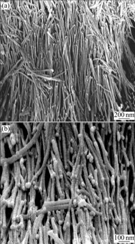
Fig.1 SEM images of alumina nanowires etched by H3PO4 and CrO3 solution: (a) Low-magnification; (b) high-magnification
TEM image in Fig.2 shows a single nanowire from AAO membrane after the first anodization. The nanowire exhibits a typical size of 50 nm in diameter and more than 1 μm in length. The chemical composition of the individual nanowire was analyzed using EDS. Fig.3 indicates that the as-prepared nanowire is composed of Al and O elements, the atomic ratio is 57.70?42.30, and the mass ratio is 69.70?30.30. A little of Al substrate may be interfused into sample before TEM characterization, so that the content of Al element is somewhat higher than that of bulk Al2O3. After the etching process, phosphoric acid solution is incompletely rinsed out and the remnant P element appears in the spectrum, or it maybe results from remnant aluminum phosphate. The C peak comes from carbon film on the TEM grids.

Fig.2 TEM image of single alumina nanowire with diameter of about 50 nm

Fig.3 EDS result of alumina nanowire
When the etching time in mixed acid solution is increased to 15 min, fewer nanowires in Fig.4 are located than that in Fig.1. Hexagonal structural cells are regularly arranged on the Al substrate, just like the honeycomb[1]. The alumina nanowires are also partly etched. In addition, the boundaries of hexagonal structure and the junctions of neighboring three hexagons can evidently be observed in Fig.4. Some alumina nanowires still attach to the corners of hexagonal structural cells on the substrate. This further proves that alumina nanowires come from the junctions of cells.
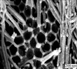
Fig.4 SEM image of Al substrate after etched in H3PO4 and CrO3 solution
3.2 Alumina nanotubes
Highly ordered porous alumina template was fabricated in the two-step anodization process. Drops of 1.0 mol/L sodium hydroxide solution were then placed on the surface. The AAO templates were partly etched. SEM images (top-view and cross-section) of alumina nanotube structure are shown in Figs.5(a) and (b), respectively. It can be clearly seen that a high yield of alumina nanotubes with uniform length and highly ordered array are formed. Alumina nanotubes also exhibit well identical orientation, parallel with each other and perpendicular to the substrate. From the top-view in Fig.5(a), each one is open to the top side and evidently it is nanotube. The cross-section image of Fig.5(b) shows that the nanotubes are independently from each other. It may be assumed that the hexagonal structures are split into individual cell and then nanotubes structure forms.
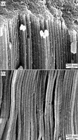
Fig.5 SEM images of alumina nanotubes etched by NaOH solution: (a) Top-view; (b) Cross-section
The TEM image of a single nanotube is shown in Fig.6. The size of nanotube is about 100 nm in diameter. The outer tube wall is very thin after being etched by NaOH. The EDS analysis in Fig.7 reveals that the nanotube consists of Al and O, and the corresponding atomic ratio is 53.20?46.80. There also are some impurity elements mixed into the sample for TEM, like Na, P and S in the spectrum.

Fig.6 TEM image of single alumina nanotube with diameter of about 70 nm
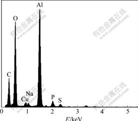
Fig.7 EDS result of alumina nanotube
3.3 Possible formation mechanism
The structural models of alumina nanostructure based on porous anodic alumina membrane are shown in Fig.8. The as-prepared porous AAO membrane(Fig.8(a)) can be schematically represented as a honeycomb structure that is characterized by a densely packed array of columnar hexagonal cells with a central pore[2]. The interface region and the junction zone of the three neighboring cells contain pure alumina, while the inner pore wall consists of contaminated alumina with acid anions[15]. Fig.8(b) shows the schematic illustration of the from-inner-to-outer etching model corresponding to the formation of alumina nanowires in the mixed solution of phosphoric acid and chromic acid, and Fig.8(c) shows the from-outer-to-inner etching model for those nanotubes formed by NaOH, respectively.

Fig.8 Structural models of AAO membrane for: (a) As- prepared; (b) After being etched in H3PO4 and CrO3 solution; (c) After being etched in NaOH solution
At the beginning, the AAO pores form almost at random positions, and hence are usually disorderedly arranged on Al surface. The nanopores in the porous layer are neither perpendicular to the Al substrate nor parallel with each other. After the first anodization for a certain time, the distribution of nanopores changes from confused to ordered. Correspondingly, the hexagonal cells at the bottom are much more regular. After chemical etching, the ordered hexagonal concaves (Fig.4) form on the Al substrate. As-prepared alumina membrane in the first anodization is made up of low ordered nanopores with different thickness of pore walls. The pore walls at the junctions of three neighboring cells are much thicker than those at the other regions. During the etching, the thinner places are dissolved first. The alumina with acid anions at inner pore walls is partly etched with pores enlarged at the same time (Fig.8(b)). At the end, pores link up so that the pore wall remained at the junction forms single nanowire[15] (Fig.1).
In general, the original alumina films of the first anodization can be chemically removed in the mixture solution of 6.0% phosphoric acid and 1.8% chromic acid during two-step anodization process[1-2]. Highly ordered AAO membrane can be obtained by a subsequently re-anodization under appropriate conditions. Therefore, excessive attention should be put on the time of removing original alumina layer, because short time (less than 30 min) etching may result in alumina nanowires and prevent the self-organized growth of porous alumina layer.
To obtain highly ordered AAO template, another anodization process should be carried out after etching for some time. Under the inducement of these honeycomb structure, porous alumina layer will be gradually organized to large-scale ordered cylindrical nanopore arrays during the second anodization, which can be used as template to fabricate nanomaterials. Obviously, the more ordered the hexagonal structure is, the higher the regularity of as-formed nanopore is. This is the fundamental of two-step anodization proposed by MASUDA et al[1]. While nanopores are well arranged with uniform thickness of pore walls, and the identical dissolution happens. Alumina nanotubes structure will be formed (Fig.5) because few drops of NaOH solution can be filled into the pores of the surface due to the surface tension, and the etch happened at interface region will result in detaching cells before the inner walls are etched as shown in Fig.8(c).
4 Conclusions
After the first anodization, alumina nanowires are successfully prepared by chemical etching porous anodic aluminum membrane in a mixture solution of 6% H3PO4 and 1.8% CrO3. At the end of the second anodization, alumina nanotubes are formed by 1.0 mol/L NaOH solution. These alumina nanostructures may be expected to have potential applications in fabrication of nanodevices.
References
[1] MASUDA H, FUKUDA K. Ordered metal nanohole arrays made by a two-step replication of honeycomb structures of anodic alumina [J]. Science, 1995, 268:1466-1468.
[2] CHICK H, XU J M. Nanometric superlattices: non-lithographic fabrication, materials, and prospects [J]. Mat Sci Eng R, 2004, 43(4): 103-138.
[3] QIN J, NOGUES J, MIKHAYLOVA M, ROIG A, MUNOZ J S, MUHAMMED M. Differences in the magnetic properties of Co, Fe, and Ni 250-300nm wide nanowires electrodeposited in amorphous anodized alumina templates [J]. Chem Mater, 2005, 17(7): 1829-1834.
[4] MIAO Z, XU D S, OUYANG J H, GUO G L, ZHAO X S, TANG Y Q. Electrochemically induced sol-gel preparation of single-crystalline TiO2 nanowires [J]. Nano Lett, 2002, 2(7): 717-720.
[5] PENG T Y, YANG H P, DAI K, PU X L, HIRAO K. Fabrication and characterization of CdS nanotube arrays in porous anodic aluminum oxide templates [J]. Chem Phys Lett, 2003, 379(5/6): 432-436.
[6] WANG Y W, ZHANG L D, MENG G W, PENG X S, JIN Y X, ZHANG J. Fabrication of ordered ferromagnetic-nonmagnetic alloy nanowire arrays and their magnetic property dependence on annealing temperature [J]. J Phys Chem B, 2002, 106(10): 2502-2507.
[7] YU M, LIU J H, LI S M. Electrochemical modification process of anodic alumina membrane [J]. Trans Nonferrous Met Soc China, 2006, 16(S2): 681-684.
[8] ZHAO Q, XU X Y, ZHANG H Z, CHEN Y F, XU J, YU D P. Synthesis and characterization of single-crystalline alumina nanowires [J]. Trans Nonferrous Met Soc China, 2005, 15(2): 306-309.
[9] WANG C W, WANG Z, LI M K, LI H L. Well- aligned polyaniline nano-fibril array membrane and its field emission property [J]. Chem Phys Lett, 2001, 341(5/6): 431-434.
[10] PU L, BAO X M, ZOU J P, FENG D. Individual alumina nanotubes [J]. Angew Chem Int Ed, 2001, 40(8): 1490-1493.
[11] ZOU J P, PU L, BAO X M, PENG D. Branchy alumina nanotubes [J]. Appl Phys Lett, 2002, 80(6): 1079-1081.
[12] PANG Y T, MENG G W, ZHANG L D, SHAN W J, ZHANG C, GAO X Y, ZHAO A W, MAO Y Q. Electrochemical synthesis of ordered alumina nanowire arrays [J]. J Solid State Electrochem, 2003, 7(6): 344-347.
[13] YUAN Z H, HUANG H, FAN S S. Regular alumina nanopillar arrays [J]. Adv Mater, 2002, 14(4): 303-306.
[14] TIAN Y T, MENG G W, GAO T, SUN S H, XIE T, PENG X S, YE C H, ZHANG L D. Alumina nanowire arrays standing on a porous anodic alumina membrane [J]. Nanotechnology, 2004, 15: 189-191.
[15] XIAO Z L, HAN C Y, WELP U, WANG H H, KWOK W K, WILLING G A, HILLER J M, COOK R E, MILLER D J, CRABTREE G W. Fabrication of alumina nanotubes and nanowires by etching porous alumina membranes [J]. Nano Lett, 2002, 2(11): 1293-1297.
[16] MEI Y F, SIU G G, FU R K Y, CHEN P, WU X L, HUANG T F, CHU P K, YANG Y. Formation mechanism of alumina nanotubes and nanowires from highly ordered porous anodic alumina template [J]. J Appl Phys, 2005, 97(3): 034305.
Foundation item: Project(BG2005009) supported by Jiangsu Provincial Hi-Tech Research Program
Corresponding author: HE Jian-ping; Tel/Fax: +86-25-52112626; E-mail: jianph@nuaa.edu.cn
(Edited by YUAN Sai-qian)

