J. Cent. South Univ. (2012) 19: 417-423
DOI: 10.1007/s11771-012-1020-7
Design of small-area and high-efficiency DC-DC converter for 1 T SRAM
LEE Jae-hyung, JIN Li-yan(金丽妍), YU Yi-ning(余忆宁), JANG Ji-hye,
KIM Kwang-il, HA Pan-bong, KIM Young-hee
Department of Electronic Engineering, Changwon National University, 9 Sarim-Dong, Changwon 641-773, Korea
? Central South University Press and Springer-Verlag Berlin Heidelberg 2012
Abstract: The direct current-direct current (DC-DC) converter is designed for 1 T static random access memory (SRAM) used in display driver integrated circuits (ICs), which consists of positive word-line voltage (VPWL), negative word-line voltage (VNWL) and half-VDD voltage (VHDD) generator. To generate a process voltage temperature (PVT)-insensitive VPWL and VNWL, a set of circuits were proposed to generate reference voltages using bandgap reference current generators for respective voltage level detectors. Also, a VPWL regulator and a VNWL charge pump were proposed for a small-area and low-power design. The proposed VPWL regulator can provide a large driving current with a small area since it regulates an input voltage (VCI) from 2.5 to 3.3 V. The VNWL charge pump can be implemented as a high-efficiency circuit with a small area and low power since it can transfer pumped charges to VNWL node entirely. The DC-DC converter for 1 T SRAM were designed with 0.11 μm mixed signal process and operated well with satisfactory measurement results.
Key words: 1 T-static random access memory; direct current-direct current converter; positive word-line voltage; negative word-line voltage; half-VDD generator
1 Introduction
Static random access memory (SRAM) integrated powers (IPs) have been used as a buffer memory for a display driver chip [1-2]. Recently, a large SRAM IP has been required as the resolution of display panel increases. For the large SRAM IP, a lot of researches have been done with a 1 T SRAM cell instead of a 6 T SRAM cell since the size of the former is about a quarter of that of the latter [3-5]. The 1 T SRAM cell consists of a transistor and a capacitor like a dynamic random access memory (DRAM) cell [6-7]. An N-type metal oxide semiconductor (NMOS) or P-type metal oxide semiconductor (PMOS) transistor can be used as the 1 T SRAM cell transistor. The NMOS transistor requires an isolated deep N-well (DNW), while the PMOS transistor has an advantage of not requiring it [8].
In the case of using a PMOS transistor and a storage capacitor of planar capacitor type in a 1 T SRAM cell, internal supply voltages are required such as positive word-line voltage (VPWL), negative word-line voltage (VNWL), bit-line precharging voltage (VBLP), positive pumping voltage (VPP), and half-VDD. The VPWL voltage is required to reduce an off-leakage through the PMOS transistor in the stand-by mode, VNWL voltage is a negative word-line voltage needed to store 0 V into the storage capacitor sufficiently by turning on the activated PMOS transistor completely, and the VBLP and VPP are half-VDD voltages. The VBLP is a voltage precharging bit-line (BL) to half-VDD in the stand-by mode and VPP is a voltage needed to reduce electric field applied to the cell plate [9]. Internal supply voltages used in the 1 T SRAM IP are all required for a small-area and low-power circuit design. In addition, the VPWL and VNWL must be designed to be insensitive to process-voltage- temperature (PVT) variation.
In this work, circuits to generate the PVT- insensitive VPWL and VNWL voltages are described by using bandgap reference current generators for respective voltage level detectors. Also, a proposed VPWL regulator and VNWL charge pump are described for a small-area and low-power circuit. In addition, the VNWL charge pump is described to raise the efficiency of transferring pumped charges to VNWL node and its implementation as a small-area and low-power circuit is also described. Furthermore, a short-circuit protection circuit preventing the pull-up and pull-down transistor from turning on is described. The DC-DC converters for 1 T SRAM are designed with 0.11 μm mixed signal process.
2 Circuit design
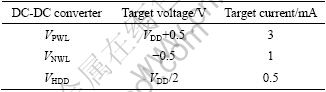
As mentioned before, it is required to have the direct current-direct current (DC-DC) converters for the PMOS transistor-type 1 T SRAM cell, as shown in Fig. 1. Table 1 gives target specifications of DC-DC converters for a wide video graphics array (WVGA)-class 1 T SRAM IP.
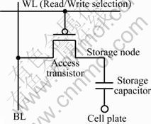
Fig. 1 1 T SRAM cell
Table 1 Target specification of DC-DC converters
In boosting the logic voltage VDD to VPWL (VPWL= VDD+0.5 V) by a charge pumping scheme [10-11], a charge bump requires a larger layout size to satisfy a large driving current of 3 mA. Thus, a VPWL regulator proposed in Fig. 2 generates a VPWL voltage.
The VREF voltage of the VPWL regulator in Fig. 2 is equal to VDD+R×IREF since a reference current flows through a resistor R. A voltage between the terminals of R and R×IREF is designed to be 0.5 V. A driving current of the common-source amplifier MP1 increases since an output voltage of a differential amplifier falls if VPWL becomes less than VREF by the differential amplifier. Then, VPWL voltage goes higher than that of VREF. If VPWL becomes higher than VREF, VPWL keeps a target voltage of (VDD+0.5 V) since MP1 turns off. An external charge reservoir capacitor is used to reduce a ripple voltage of the VPWL.
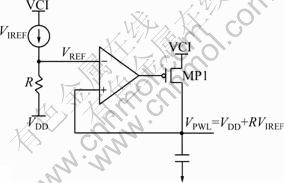
Fig. 2 Proposed VPWL regulator
Figure 3 shows a designed bandgap reference current generator using parasitic NPN-type bipolar junction transitions (NPN BJTs) with a logic process of not requiring low-VT transistors [12]. A differential amplifier is biased by a self-biasing circuit consisting of MN2, MN3 and MP2. A constant temperature-insensitive current flown by Q0, Q1, R1, and R2 can be made insensitive to a PVT variation by a cascode mirror with a wide swing consisting of MP3, MP4, MP5, MN6 and MN7. This reference current becomes IREF in Eq. (1) by mirroring:
 (1)
(1)
where VT (=kT/q) is a thermal voltage; VBE0 is a voltage between the emitter and the base of an NPN BJT Q0.
A block diagram of VNWL generator generating a negative word-line (WL) voltage is complementary to that of the conventional VPWL generator in structure in order to store a full VSS by turning on the PMOS access transistor of 1 T SRAM cell. As shown in Fig. 4(a), it consists of a bandgap reference current generator, a VNWL level detector, a ring oscillator, a control logic, two stages of charge pumps and a VSS precharge circuit. Also, an external charge reservoir capacitor was used to reduce a ripple voltage of the VNWL generator. Figure 4(b) shows a voltage bias circuit of cascode current mirror type using a sink current source IREF to supply a bias voltage to the VNWL level detector. The VNWL level detector is shown in Fig. 4(c) and VNWL generator enables VNWL_EN signal to go high in the case that VNWL voltage is higher than a target voltage. Then, the ring oscillator oscillates and the charge pump operates. In contrast, VNWL_EN signal switches low and pumping stops if VNWL voltage is less than a target voltage.
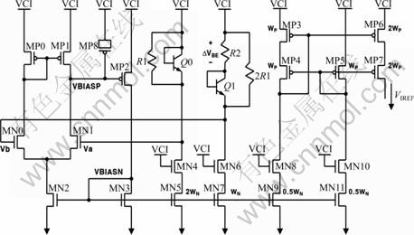
Fig. 3 Reference current generator
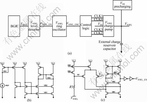
Fig. 4 VNML generator scheme: (a) Block diagram of VNWL generator; (b) VNWL voltage bias circuit; (c) VNWL level detector
As shown in Fig. 5, the conventional negative charge pump [13] consists of two precharge control circuits (MP3 and MP4; MP5 and MP6), PMOS charge transfer switches (MP1 and MP2), cross-coupled NMOS charge transfer switches (MN1 and MN2), charge pumping MOS capacitors (MP7, MP8, MP9, and MP10). Gate nodes of the NMOS charge transfer switches N3 and N4 switch between -0.5 and 0 V in the steady state in the case that a target voltage of the VNWL is -0.5 V. Then, the on currents of the switches are small since the maximum voltage difference between the gate and the source is 0.5 V. In addition, there is a limit in reducing the oscillation period of the ring oscillator to increase a driving current.
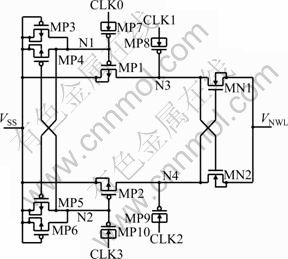
Fig. 5 Conventional VNWL charge pump
Figure 6(a) shows a proposed VNWL charge pump circuit. The charge pump consists of two precharge control circuits (MP3 and MN7; MP4 and MN10), NMOS charge transfer switches (MN8 and MN9), cross- coupled charge transfer switches (MN1 and MN2), body-potential biasing circuits (MN3 and MNP4; MNP5 and MN6), and charge pumping MOS capacitors (MP1 and MP2). The body potential of each NMOS charge transfer switch protects its threshold voltage from increasing due to a body effect by connecting its body potential to its source node electrically using its body-potential biasing circuit. Charge pumping occurs two times per cycle and four signals (CLK0, CLK1, CLK2 and CLK3) are non-overlapping clocks swinging between 0 V and VCI voltage. Figure 6(b) shows each node voltage waveform of the VNWL charge pump in the steady state. The N1 and N2 node voltages in the steady state swing between VNWL and VCI voltage by the precharge control circuits and the charge pumping MOS capacitors. Since node voltages of N1, N2, N3 and N4 during an interval of t4 are VNWL, VCI voltage, VNWL and VSS, respectively, MN1 turns on, MN2 turns off, and node voltage of N4 precharges to VSS. Then, negative charges of node N3 boosted to VNWL are transferred to the output node through MN1 completely. In addition, boosted negative charges of node N4 during an interval of t1 are transferred to the output node through MN2. Then, there is an advantage that negative charges can be transferred completely due to a large voltage difference between the gate and source of each NMOS charge transfer switch since the gate node of the NMOS charge transfer switch swing between 0 V and VCI voltage.
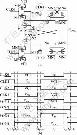
Fig. 6 Proposed VNML charge pump scheme (a) and its timing diagram in steady state (b)
A half-VDD voltage generator is used to supply a precharging voltage of VDD/2 to the cell plate and BL of 1 T SRAM cell. As shown in Fig. 7, the conventional half-VDD voltage generator consists of a voltage divider, a bias stage, a push-pull current-mirror amplifier, an output stage with an NMOS pull-up and a PMOS pull-down transistor [14]. The maximum pull-up current is proportional to (VDD/2-VTN)2 and the maximum pull- down current to (VDD/2-|VTP|)2b. The conventional circuit has a disadvantage that the driving capacity of the NMOS pull-up transistor falls and its operating characteristic worsens if a supply voltage VDD decreases.
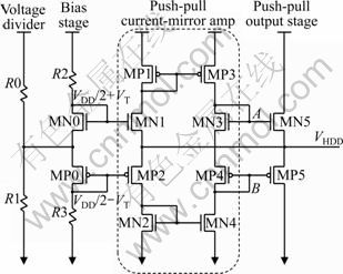
Fig. 7 Conventional half-VDD generator
As shown in Fig. 8, a designed half-VDD voltage generator consists of two differential amplifiers (DIFF0 and DIFF1), a short-circuit current protection circuit, a PMOS pull-up transistor (MP0) and an NMOS pull-down transistor (MN0) [15]. Thus, it has a push-pull structure of a low stand-by and high driving current. We design it such that a pull-up current is proportional to (VDD-|VTP|)2 using the PMOS pull-up transistor and a pull-down current to (VDD-VTN)2 using the NMOS pull-down transistor. Also, there exists a dead zone of 30 mV between VREFL and VREFU by a class AB design since a short-circuit current increases if the pull-up and pull-down currents increase. VDD can keep VDD/2 voltage since the output voltage VHDD is pulled up by the pull-up transistor if it is less than VREFL voltage and is pulled down by the pull-down transistor if it is higher than VREFU voltage. Also, the short-circuit protection circuit can prevent the short-circuit current by removing a simultaneously turned-on interval of both MN0 and MP0 with offsets of the differential amplifiers.
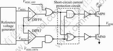
Fig. 8 Designed half-VDD generator
3 Simulation results
Major design specifications of the designed DC-DC generators for 1 T SRAM with 0.11 μm mixed signal process, such as the output voltages and driving currents, are listed in Table 1.
A simulation result of generating an output voltage of VDD+0.5 V in the VPWL generator using VCI voltage is shown in Fig. 9. The results show that the output signal VPWL is a stable voltage which simulates under the conditions that temperature are -40, 25 and 85 °C; and all corner models of transistors. Figure 9(a) shows a simulation result of VPWL output with respect to a VCI voltage variation at VDD voltage of 1.2 V, and Fig. 9(b) shows that with respect to a VDD variation over VCI voltages from 2.5 V to 3.3 V. The output voltages of the VPWL generator are from 1.69 to 1.71 V at VDD of 1.2 V for both cases. Also, it can be seen from the simulation that the designed VPWL generator has an output voltage of VDD+0.5 V and a current driving capacity of 3 mA, as shown in Fig. 9(c).
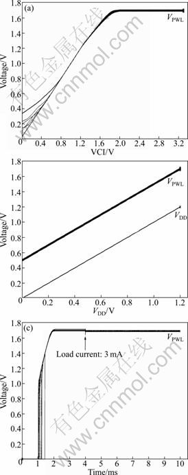
Fig. 9 Simulation result of VPWL generator
Figure 10 shows a simulation result of transferred amounts of charges with respect to the pumping periods of the proposed charge pump compared with the conventional counterpart in the VNWL generator. Normalized transfer charge (NTC) means pumping charges transferred to the output node with a given oscillation period normalized by those with a sufficiently long oscillation period. According to the simulation result, the proposed charge pump has a better characteristic of charge transfer than the conventional counterpart under the following conditions: VCI voltage of 2.5 V, temperature of 85 °C, and slow models of NMOS and PMOS transistors.
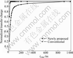
Fig. 10 NTC graph of VPWL charge pump with respect to pumping periods
Figure 11 shows a VNWL output voltage of -0.5 V under the following conditions: a supply voltage (VCI) of 2.5 V, temperature of 85 °C, and slow models of NMOS and PMOS transistors. Also, the settling times, ripple voltages and driving currents of the VNWL output voltage are listed in Table 2. The output has the maximum ripple voltage of 43.5 mV and a driving current of more than 1 mA in the case of no load current.
A simulation for a half-VDD voltage generator is implemented under the following conditions: a supply voltage (VDD) of 1.08 V, temperature of 85 °C, and slow models of NMOS and PMOS transistors. The simulation results are shown in Fig. 12. Figure 12(a) shows a driving current variation IVHDD with respect to an output variation VHDD. The driving current is 500 μA. The generator keeps VDD/2 voltage by pull-up and pull-down current when it is out of the dead zone of ±15 mV at a voltage of VDD/2. Figure 12(b) shows a result of the settling times of the half-VDD generator at power-up. It takes 25 μs for the output voltage VHDD to go up to VDD/2. Thus, the designed half-VDD voltage generator can be used in the LCD driver IC since the required settling time is from 100 μs to 200 μs.
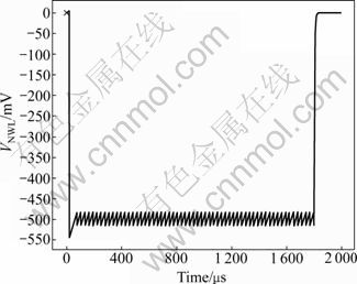
Fig. 11 Simulation result of VNWL generation
Table 2 Settling times, ripple voltages and driving currents of VNWL under different simulation conditions
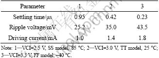
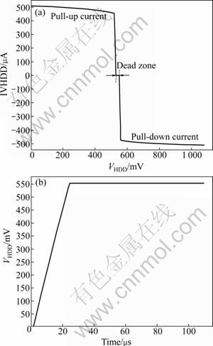
Fig. 12 Simulation results: (a) IVHDD vs VHDD; (b) Settling time of half-VDD voltage generator at power-on
Layout images of the designed DC-DC converters for 1 T SRAM with 0.11 μm mixed signal process are shown in Fig. 13. Layout sizes of the VPWL generator in Fig. 13(a), VNWL generator in Fig. 13(b), and half-VDD generator in Fig. 13(c) are 340.96 μm × 70 μm, 522.63 μm × 70 μm and 64.16 μm × 70 μm, respectively.
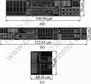
Fig. 13 Layout image of designed DC-DC conventional for 1 T SRAM: (a) VPWL generator; (b) VNWL generator; (c) Half-VDD generator
4 Conclusions
1) A DC-DC converter is designed for 1 T SRAM. A VPWL generator is proposed, which generates VDD+0.5 V using VCI voltage in the LCD driver IC to turn off the PMOS access transistor of 1 T SRAM cell and to reduce a leakage current.
2) A VNWL generator is proposed which generates a negative word-line voltage to store the capacitor of 1 T SRAM cell to the full VDD. In addition, the driving current is increased by making the gate node of the NMOS charge transfer switch swing to VCI voltage for the negative charge pump compared with the conventional charge pump.
3) A half-VDD voltage generator is designed, increasing the driving current and protecting a short- circuit current to precharge the cell plate and BL voltage of the 1 T SRAM cell to VDD/2 voltage. It is confirmed by the computer simulation that the designed DC-DC converters can meet the design specifications.
Acknowledgements
This research is financially supported by Changwon National University in 2011-2013.
References
[1] KIM B S, KIM Y G, HONG S Y. Low power 260k color TFT LCD one-chip driver IC [C]// Proceedings of 5th International Symposium on Quality Electronic Design. San Jose: USA, 2004: 126-130.
[2] XIAO Weng-yu, CHEN Zhi-liang. A mixed-signal driver chip for 65k-colr passive-matrix OLED [C]// Proceedings of 6th International Conference on ASIC. Shanghai: China, 2005: 473-477.
[3] LEE J H, JEON H G, KIM K I. Design of a redundancy control circuit for 1T-SRAM repair using electrical fuse programming [J]. J the Korean Institute of Maritime Information and Communication Sciences, 2010, 14(8): 1877-1886. (in Korean)
[4] KWON O S, MIN K S. Dataline redundancy circuit using simple shift logic circuit for dual-port 1T-SRAM embedded in display ICs [J]. Institute of Korean Electrical and Electronics Engineers, 2007, 11(4): 129-136. (in Korean)
[5] CHA S R, LEE B S, KIM H Y, CHOI H Y. Design of graphic memory for QVGA-Scale LCD driver IC [J]. The Institute of Electronics Engineers of Korea, 2008, 31(1): 589-590. (in Korean)
[6] LEUNG W, HSU F, JONES M E. The ideal SoC memory: 1T-SRAM [C]// Proceeding of 13th annual IEEE international ASIC/SoC Conference. Arlington: USA, 2000: 32-36.
[7] SOMASEKHAR D, LU S L, BLOECHEL B, LAI K, BORKAR S, DE V. Planar 1T-Cell DRAM with MOS storage capacitors in a 130 nm logic technology for high density microprocessor caches [C]// Proc ESSCIRC. Firenze: University of Pavia, 2002: 127-130.
[8] CHWANG R, CHOI M, CREEK D, STERN S, PELLEY P, SCHUTA J, BOHR M, WARKENTIN P, YU K. A 70ns high density CMOS DRAM [C]// Proceeding of Solid-State Circuits Conference. New York: USA, 1983: 56-57.
[9] LU N C C, CHAO H H. Half-VDD bit-line sensing scheme in CMOS DRAM’s [J]. IEEE Journal of Solid-State Circuit, 1984, 19(4): 451-454.
[10] CHO S I, LEE J H, PARK H J, LIM G H, KIM Y H. Two-phase boosted voltage generator for low-voltage DRAMs [J]. IEEE Journal of Solid-State Circuit, 2003, 38(10): 1726-1729.
[11] KIM T H, LEE J H, HA P B, KIM Y H. A VPP Generator Design for a Low Voltage DRAM [C]// C. the Korean Institute of Maritime Information and Communication Sciences. Busan: Korea, 2007: 776-780. (in Korean)
[12] LEE T Y, LEE J H, KIM J H, SHIM O Y, KIM T H, PARK M H, HA P B, KIM Y H. A bandgap reference voltage generator design for low voltage SoC [J]. Journal the Korean Institute of Maritime Information and Communication Sciences, 2007, 12(1): 137-142. (in Korean)
[13] KIM Y H, PARK H J, SOHN J D, CHOI J S, PARK C S, AHN S H, JEONG J Y. Two-phase back-bias generator for low-voltage Gigabit DRAMs [J]. IEEE Electronic Letters, 1998, 34(19): 1831-1833.
[14] NAKAGOME Y, TANAKA H, TAKEUCHI K, KUME E, WATANABE Y, KAGA T, KAWAMOTO Y, MURAI F, IZAWA R, HISAMOTO D, KISU T, NISHIDA T, TAKEDA E, ITOH K. An experimental 1.5-V 64-Mb DRAM [J]. IEEE Journal of Solid-State Circuit, 1991, 26(4): 465-472.
[15] LEE J H, WOO E C, KANG H G, LIM G H, HA P B, KIM Y H. A Half-VDD Voltage generator for low-voltage DRAM [C]// Korean Conference on Semiconductor. Seoul: KCS, 2005: 523-524. (in Korean)
(Edited by DENG Lü-xiang)
Foundation item: Work supported by the Second Stage of Brain Korea 21 Projects
Received date: 2011-04-26; Accepted date: 2011-10-10
Corresponding author: KIM Young-hee, Professor, PhD; Tel: +82-55-285-1023; E-mail: youngkim@changwon.ac.kr

