�������Թ�����ѹ�յ���ͭ����� �ݶ�����/�ṹ
��Դ�ڿ����й���ɫ����ѧ��(Ӣ�İ�)2014���2��
�������ߣ��� � �� ΰ �� �� �����
����ҳ�룺441 - 448
�ؼ��ʣ���ѹ����ͭ���ݶ�����/�ṹ����������
Key words��burnishing; pure copper; gradient nano/micro-structure; surface nanocrystallization
ժ Ҫ��Ϊ���о��ɾ������Թ�����ѹ�ڴ�ͭ�����յ������ݶ�����/�ṹ�������侧��ϸ�����ƣ�����SEM��TEM��XRD��OM�ȷ����۲���Ʒ����治ͬ��ȵ���֯�ص�Ͳ������ԡ������������ѹ��������� ��/�ṹ���ȳ���100 ��m���������Ӳ������������ߣ�������ھ����ߴ�ļ�С�������ɵĵ�������Ϊ�������ȡ���Ҿ����������ΪС�ǶȾ��硣�־�ͨ��λ���˶�ϸ�������ף������������γ���������Ҫ���������ṹ���γ���λ���˶�����������ֲ�����ľ�����ת��
Abstract: In order to investigate a gradient nano/micro-structured surface layer on pure copper produced by severe plasticity roller burnishing (SPRB) and grain refinement mechanism, the microstructure characteristics and material properties of sample at various depths from the topmost surface were investigated by SEM, TEM, XRD, OM etc. The experimental results show that the gradient nano/micro-structure was introduced into the surface layer of over 100 ��m in thickness. The remarkable increase in hardness near the topmost surface was mainly attributed to the reduced grain size. The equiaxed nano-sized grains were in random orientation and the most of their boundaries were low-angle grain boundaries (LAGBs). The coarse grains are refined into the few micro-sized grains by dislocation activities; deformation twinning was found to be the primary form for the formation of submicron grains; the formation of nanostructure was dominated by dislocation activities accompanied with rotation of grains in local region.
Trans. Nonferrous Met. Soc. China 24(2014) 441-448
Jing ZHAO, Wei XIA, Ning LI, Feng-lei LI
National Engineering Research Center of Near-net-shape Forming Technology for Metallic Materials, South China University of Technology, Guangzhou 510640, China
Received 28 January 2013; accepted 12 September 2013
Abstract: In order to investigate a gradient nano/micro-structured surface layer on pure copper produced by severe plasticity roller burnishing (SPRB) and grain refinement mechanism, the microstructure characteristics and material properties of sample at various depths from the topmost surface were investigated by SEM, TEM, XRD, OM etc. The experimental results show that the gradient nano/micro-structure was introduced into the surface layer of over 100 ��m in thickness. The remarkable increase in hardness near the topmost surface was mainly attributed to the reduced grain size. The equiaxed nano-sized grains were in random orientation and the most of their boundaries were low-angle grain boundaries (LAGBs). The coarse grains are refined into the few micro-sized grains by dislocation activities; deformation twinning was found to be the primary form for the formation of submicron grains; the formation of nanostructure was dominated by dislocation activities accompanied with rotation of grains in local region.
Key words: burnishing; pure copper; gradient nano/micro-structure; surface nanocrystallization
1 Introduction
Owing to the extraordinary mechanical and physical properties of surface nanocrystallization (SNC) materials [1,2], numerous SNC techniques have been proposed. Among these techniques, surface self-nanocrystallization (SSNC) techniques gradually attract great interests of researchers since they can utilize the traditional surface processing techniques to fabricate SNC materials without considering the adhesion force between the nanocrystalline surface layer and matrix [3]. Most SSNC techniques rely on multidirectional or monotonic high-speed impact on the sample surface to refine coarse grains into nano-sized grains, such as surface mechanical attrition treatment (SMAT) [4-6], high energy shot peening (HESP) [7], ultrasonic shot peening (USSP) [8], ultrasonic surface processing (USER) [9]. Nevertheless, the poor surface qualities of the treated surface layer hinder the extensive industrial application. It is worth noting that LU et al [10] have synthesized a gradient nano/micro-structure in the surface layer on copper, by the surface mechanical grinding treatment (SMGT) in recent years. The treated nano-sized copper would become an ideal engineering material because of its high strength and good tensile plasticity [11]. However, the usage of liquid nitrogen cooling to avoid grain recovery and/or recrystallization is not suitable for industrial production. In short, difficulty in finding an easy-implementation and low-cost SSNC technique is a main obstacle for industrial application and development of SNC metals and alloys.
Burnishing, similar with SMGT, has a processing way of repetitive extrusion on material surface, which makes it possible to fabricate the gradient nano/micro- structured surface layer. In fact, recent investigation has demonstrated that Mg alloy with a gradient ultrafine-grain surface layer was produced using cryogenic burnishing [12]. In our work, a new SSNC technique based on burnishing is proposed, named severe plasticity roller burnishing (SPRB), which has produced a gradient nano/micro-structure on copper successfully at room temperature. This newly developed technique has a promising prospect in industrial application than SMGT since it achieved the gradient nano/micro-structured surface layer only by an ordinary lathe and a simple burnishing tool. The microstructural evolution mechanism and the formation of gradient nano/micro- structure involved in SPRB are essential and crucial issues to help us to understand the properties of SNC material induced by SPRB more comprehensively.
The strain-induced microstructure evolution and the refinement mechanism of SSNC process have been of great concern in the past decades. The diversity of the plastic deformation mode caused by various techniques and materials affects the behavior and microstructural evolution of nanostructured materials [3]. So the obvious difference in plastic deformation mode between impact- typed SSNC and extrusion-typed SSNC definitely causes the distinction on deformation mechanism and microstructure characteristics. For example, the fibrous structure in the plastic deformation layer is not seen in SMAT [5], but is common seen in SMGT [10]. However, most investigations on deformation mechanism of SSNC processes are based on the impact-typed SSNC techniques, but little work has been reported on the mechanism underlying the grain refinement of the extrusion-typed ones up to now.
The objective of the present work is to study the grain refinement mechanism involved in SPRB by the microstructure features of gradient nano/micro- structured surface layer on copper at different depths from the top surface. The surface performance improvement of the deformation layer including surface roughness and hardness is also our concern.
2 Experimental
A rod sample with dimensions of d40 mm��10 mm was attained from a pure copper (99.97% in mass fraction) bar for SPRB. The initial grain size of the sample was about 75 ��m. In order to increase the pressure induced by burnishing tool, a boss (1 mm in width and 6 mm in height) was machined on the end face of the sample at a feed rate of 0.12 mm/r and a spindle speed of 560 r/min under oil lubrication (SAE10W-30).
Figure 1(a) gives the experimental set-up of SPRB. The process was conducted on a C6132A1 lathe. A designed tool with 5 equally distributed rollers (d6 mm��8 mm), made of YG-8 cemented carbide, was used. An S-type pressure sensor was connected with the lathe to obtain the real-time radial burnishing force (Fr). The sensor signal was acquired through the Advantech USB-4711A DAQ card and processed on PC. Before SPRB, the burnishing tool was clamped on the lathe tailstock and applied a given preload on the boss. When the SPRB began, the roller rotated at a high speed to decrease the height of boss rapidly, as shown in Fig. 1(b). The process was time-controlled with the duration of 90 s per pass. The process was conducted at a spindle speed of 560 r/min and a burnishing load of 2100 N 8 passes under oil lubrication (SAE10W-30) at room temperature. The height of boss was finally reduced to ~1 mm. The stain rate was estimated at 102-103 s-1 in the top surface layer of the sample [13].
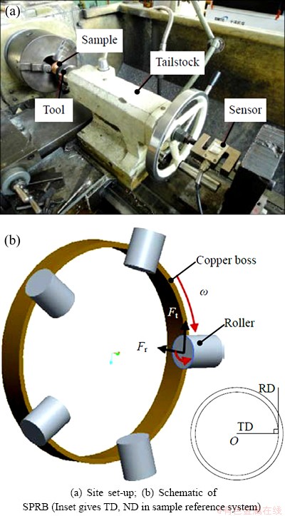
Fig. 1 Experimental set-up
The sample was polished with carbide papers to the specified depths, measured by displacement sensor OD5-25W01 at a resolution of 0.02 ��m. The microstructural evolution at different depths was characterized by an optical microscope (OM, Leica DM1500) and scanning electron microscope (SEM, Nano 430). The top surface of sample was investigated by a transmission electron microscope (TEM, JEOL 3010). The X-ray diffraction (XRD, Rigaku D/max 2500PC X-ray diffractometer) measurement was carried out at 40 kV and 150 mA using Cu K�� radiation on the RD-TD plane of sample, as shown in Fig. 1(b). The surface roughness improvements of the sample were measured by a BMT Expert 3D measurement system. The microhardness at each depth was determined by a HVS-1000 Vickers hardness testing machine, with a load of 4.9 N and a loading time of 20 s. The mean value was determined from the values around a mark point. The grain size distribution was a statistical result of 200 grains selected randomly from Fig. 5. A pair of orthogonal lines were drawn through the long axis and short axis of a grain. The pixel lengths of long axis and short axis were read and converted into the real lengths.
3 Results
3.1 Microstructure
3.1.1 Cross-sectional observations
The cross-sectional SEM observation of the sample is shown in Fig. 2. It can be seen that a gradient structure forms in the surface layer, representing the strain decrease from the maximum at the topmost surface to zero in the matrix. The grain boundaries of the top layer (depth<100 ��m) could hardly be identified, which indicates that severe plastic deformation occurs in the top layer during SPRB. It is worth mentioning that the gradient structure is similar with the one observed after SMGT [10], but is more uniform compared with latter at the same depth. The thickness of the deformation layer is about 600 ��m, which is twice that by SMAT for 5 min [5].

Fig. 2 SEM image showing cross-section of sample
In order to investigate the grain refinement process involved in SPRB, microstructure characterizations of sample at different depths from the topmost surface, marked by h0-h6 in Fig. 2, were conducted.
3.1.2 Microstructure characteristics of deformation layer
Figure 3(a) shows that the grains at h6 have no obvious deformation, and the grain boundaries are straight, which can be defined as the matrix. With increasing the deformation strain at h5, as shown in Fig. 3(b), the grains are elongated slightly and some grain boundaries are blurred and curved. At h4, fiber structures form along burnishing direction, leading to the segmentation of coarse grains. The refinement degree of the coarse grains is significantly different. The grain refinement in some regions is faster than other regions. For example, equiaxed grains with size of ~5 ��m marked with arrows in Fig. 3(c), are quite smaller than ones in other regions.
It is well recognized that the degree of etch is same for the same lattice plane of a material, so we define two types of regions in Figs. 3(d)-(f): bright (a region labeled with ��B�� in Fig. 3(d)) and dark (a region labeled with ��D�� in Fig. 3(d)) regions, to reveal the evolutions of microstructure and grain orientation. The grains in dark regions are smaller than the ones in bright regions (Fig. 3(d)), indicating that the dark regions are of newly generated fine-grained structure. The grain orientations of dark regions are approximate with those of the preferential refinement regions in Fig. 3(c). It can be observed that the total area ratio of the dark regions to the bright ones increases with decreasing the depths from the top surface (Figs. 3(e)-3(f)). These findings indicate clearly that the dark regions play an important role in the grain refinement.
It can be concluded that the grain orientations of dark regions are preferential at h1 from Fig. 3(f). Texture analysis gives more details of grain orientation to reveal the formation of submicron grains. The deformation textures were determined from the (200), (220), (111) and (311) pole figures. The experimental data were processed to obtain the orientation distribution function f(g) (ODF). The ��2=0, 45�� sections of ODF for the samples before and after SPRB are shown in Fig. 4. The XRD measured depth is about 30 ��m from the topmost surface of sample. The textures before SPRB consist of components like {001}<110> rotated cube (RC), {110}<001> Goss (G), {110}<110> rotated Goss (RG) and {114}<221> (GT), which is the ideal twin orientation of goss. The ODF of the burnished sample shows an orientation density increase around the RG component while other components existing before SPRB almost disappear. The strength of {114}<110> (RGT), the ideal twin orientation of the rotated Goss, is roughly equal to that of RG component after SPRB.
SPRB can be simplified in the form of tension along TD and compression along ND, so the Schmid factor m can be expressed as [14]
 (1)
(1)
where �� is the angle between TD direction and slip/twin direction; �� is the angle between TD direction and the normal of slip/twin plane; �� is the angle between ND direction and slip/twin direction; d is the angle between ND direction and the normal of slip/twin plane. According to Eq. (1), the Schmid factors (SF) for slip/twin systems of the components existing before and after SPRB are calculated. The maximum Schmid factors for slip/twin systems and the corresponding number of active slip/twin systems having the maximum SF are listed in Table 1.
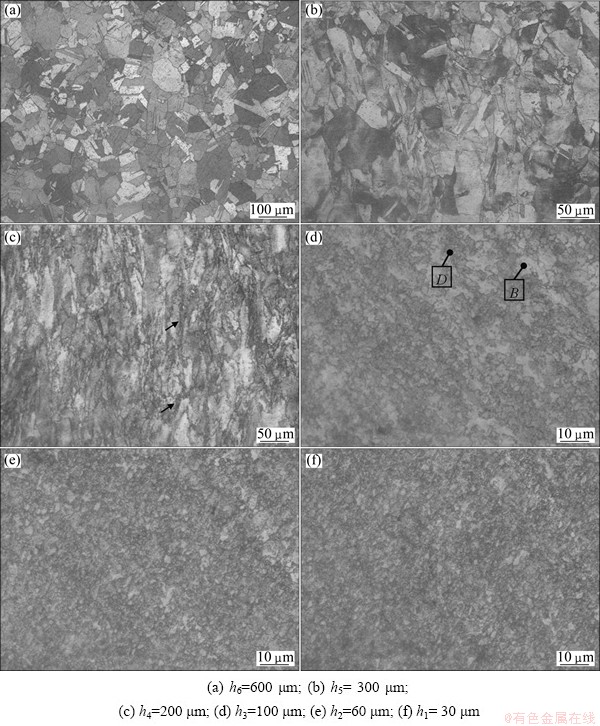
Fig. 3 OM images showing microstructures of sample at different depths from topmost surface
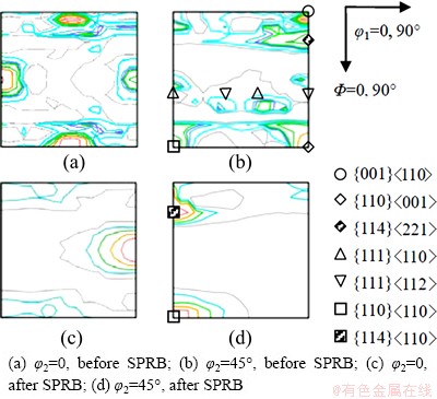
Fig. 4 ODF representing textures of samples before SPRB (Imax=2.4; level=0.45, 0.46, 1.00, 1.30, 1.60, 1.80, 2.10) and after SPRB (Imax=4.8; level=0.00, 1.00, 1.80, 2.50, 3.30, 4.00)
Table 1 The maximum Schmid factors Mmax for slip systems and twin systems and corresponding numbers of active slip systems and twin systems during SPRB

Larger SF of component means that the grain with this orientation is easier to deform, which can promote the grain refinement. The RG, RGT and RC have the largest SF for twin systems shown in Table 1, which is consistent with the texture results of the burnished sample. Assume that the critical resolved shear stress for slip is equal to that for twinning. The results show the onset of twinning is easier than dislocation slip for the three components. The twinning relation between RG and RGT indicates that part of RGT component evolves from RG component. Meanwhile, the strength values of two components are almost the same. It can be concluded that most grains are in the form of twins. Besides, the Schmid factors for slip systems of these three components are also high, which means that the dislocation slipping is also activated and works together with the twinning in microstructural evolution. It should be noticed that XRD has a certain penetration depth for a given material. The penetration depth of copper is verified as 19 ��m by Beer�CLambert law, so the texture measured is an average value in the range of 30-50 ��m depth from the topmost surface.
In the top surface, the microstructure is characterized by nano-sized grains from TEM observations (Fig. 5). The corresponding selected-area electron diffraction (SAED) pattern shown in Fig. 5 indicates that randomly oriented grains are obtained by SPRB. The grain size distributions of long axis and short axis confirm to the normal logarithmic distribution approximately (Fig. 6). The average long axis grain size (dl) and short axis grain size (ds) are 11 and 8 nm respectively. So the nano-sized grains can be fairly considered being equiaxed with the (dl/ds) of 1.2.

Fig. 5 Bright field image of top surface of burnished copper
3.1.3 Region definition of gradient nano/micro- structured surface layer
The grain size distributions at h0-h3 are shown in Fig. 7. The error bars for the arithmetic mean that values of grain sizes are calculated. The arithmetic mean values of grain size get smaller when the depth is close to the topmost surface, which indicates that the grain refinement is more uniform in the top surface. The grain size of short axis at h1 is partly in the nanometer range, so the SNC layer is defined as 0-30 ��m. The average size of short axis at h3 is out of 1000 nm, so the sub-micron layer is defined as 30-100 ��m. In short, the thickness of the gradient nano/micro-structured surface layer is about 100 ��m from the topmost surface, which is much larger than that in Ref. [15].

Fig. 6 Grain size distributions of long axis (dl) (a) and short axis (ds) (b) in top surface (Inset gives the ratio of dl/ds)
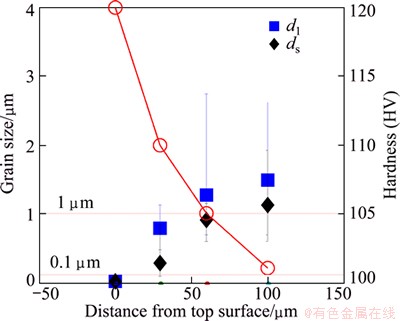
Fig. 7 Grain size distributions at h0, h1, h2, h3 and corresponding hardness values
3.2 Improvement on surface properties of deformation layer
SPRB improves the surface quality greatly because the surface roughness (Ra) decreases from (1.5��0.35) ��m to (0.56��0.04) ��m after SPRB.
The hardness increases from HV68 in the matrix to HV 120 in the top surface. The hardness at the topmost surface is about 1.76 times that of the matrix, which is lower than the hardness of SMGT copper [5]. The nano-sized twins have been proven to have the higher hardness [16]. However, few twins are found in the topmost surface in the burnished sample (hereafter referred in discussion). So it may explain the difference in hardness between two techniques. The hardness within 100 ��m from the topmost surface is greater than HV 100, as indicated in Fig. 8. The relationship between hardness and d-1/2 (d is the average grain size) in this range is examined, as shown in Fig. 8. The result shows that it is consistent with the Hall-Petch relationship. The slope in the nanometer scale is different from the one out of the nanometer size range, which can be explained that the Hall-Petch relationship becomes temperature-dependent and size-dependent when the grain size of crystals is less than 100 nm [17].

Fig. 8 Variation of hardness with distance from top surface (Inset gives the relationship between hardness and d-1/2)
4 Discussion
The increasing strain and strain rate from the topmost surface to matrix play a key role in fabricating the gradient nano/micro-structured surface layer induced by SPRB technique. Based on the features of the gradient microstructure, the mechanisms of grain refinement are discussed at different depths.
Copper is a FCC crystal with medium stacking fault energy (78 mJ/m2). It has been observed that slipping is the prevalent deformation mode at a low strain level [5]. In the micron layer, slipping is hard for the grains with ��hard�� orientations, leading to the formation of dislocations in the interior of grains. The dislocation multiplication helps to form some dislocation areas with a certain length. Only narrow and long deformed regions generate in some local areas (Fig. 3(c)) since the number of activated slip systems is few at a low strain level. The new grains/sub-grains are formed in these areas probably through continuous dynamic recrystallization (DRX) to release the energy localization [18]. With the increase of strain, more grains turn to have ��hard�� orientations, so the dislocation intensity increases and the dislocation areas cover wider, as shown in Fig. 3(d), which propels the formation of dislocation walls (DDWs) to refine the grains to a few microns.
Texture results reveal that the submicron grains are mostly in the form of twins in the range of 30-50 ��m depth. So the increasing strain will give rise to the onset of twins. It is worth noting that this microstructural feature is very similar to the formation of twin lamellae in the SMAT of polycrystalline copper [5], which indicates that the deformation twinning is the predominant refinement mechanism to form the submicron grains. It has been shown that the existence of deformed twins is evidenced by the RGT and RG components are preferred orientations under SPRB.
In order to reveal the formation of nanograins (depth 0-30 ��m), another TEM image (Fig. 9) with a low magnification in the top surface is given. The dislocation tangles can be seen in region A (marked by the white dotted ellipse) and the dislocation walls (DDWs) with parallel structure are also found as the white arrows in region B, which reveal that dislocation activities play a key role in refining grains to the nanometer scale. This is confirmed by a high resolution TEM image shown in Fig. 10. It is widely recognized that the low-angle grain boundary consists of a series of dislocations. Most grains in Fig. 10 have low-angle grain boundaries (LAGBs), namely, grain A has a small misorientation with the surrounding grains, which proves the existence of dislocations at the grain boundaries. The dislocations and/or stacking faults are found in the interior of grain H (Fig. 10(a)) by inverse fast Fourier transform (IFFT), indicating that the dislocations will trigger the formation of nanograins. Some equiaxed grains have high contrast relative to the surrounding grains (e.g. the grains marked by dark arrows in Fig. 9). It is an evidence to support the rotation of grains occurring during the formation of the equiaxed grains [19]. Almost no evidence of twining relationship was identified in HRTEM image (Fig. 10). Therefore, deformation twinning may not be a major formation mechanism of nanosized grains.
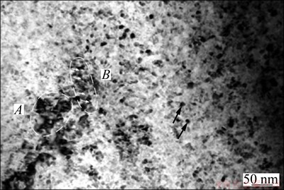
Fig. 9 TEM observation in low magnification
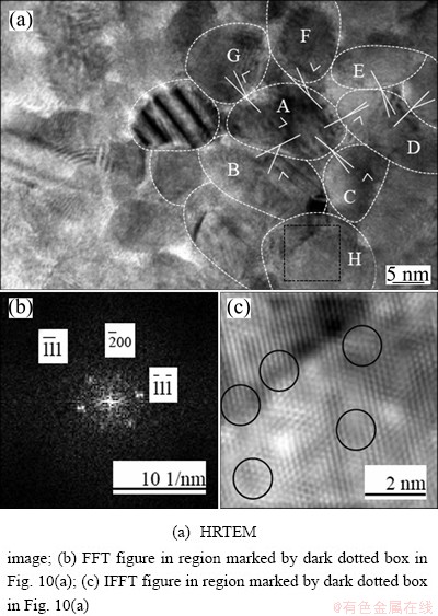
Fig. 10 HRTEM observations in top surface
5 Conclusions
1) A gradient nano/micro-structured surface layer was fabricated using a new SPB technique on pure copper. The average grain size of equiaxed nano-sized grains with low-angle grain boundaries (LAGBs) is about 10 nm. The thickness of the gradient nano/micro- structured surface layer is ~100 ��m.
2) The formation of the equiaxed nano-sized grains is mainly dominated by dislocation activities accomplished with the rotation of grains.
3) A strong texture consisting of rotated Goss and twin of rotated Goss components reveals that deformation twinning is the primary microstructural evolution mechanism for the formation of submicron grains.
4) The coarse grains are refined into the few micro-sized grains by dislocation activities.
5) The surface properties of copper by SPRB are enhanced obviously. The hardness of topmost surface is 1.76 times that of the matrix. The roughness decreases from 1.5 ��m to 0.56 ��m after SPRB.
References
[1] TONG W P, TAO N R, WANG Z B, LU J, LU K. Nitriding iron at lower temperatures [J]. Science, 2003, 299: 686-688.
[2] ZHANG Y S, HAN Z, LU K. Fretting wear behavior of nanocrystalline surface layer of copper under dry condition [J]. Wear, 2008, 265: 396-401.
[3] XU Bing-shi. Nano surface engineering [M]. Beijing: Chemical Industry Press, 2004. (in Chinese)
[4] SUN H Q, SHI Y N, ZHANG M X, LU K. Plastic strain-induced grain refinement in the nanometer scale in a Mg alloy [J]. Acta Materialia, 2007, 55(3): 975-982.
[5] WANG K, TAO N R, LIU G, LU J, LU K. Plastic strain-induced grain refinement at the nanometer scale in copper [J]. Acta Materialia, 2006, 54(19): 5281-5291.
[6] TAO N R, WANG Z B, TONG W P, SUI M L, LU J, LU K. An investigation of surface nanocrystallization mechanism in Fe induced by surface mechanical attrition treatment [J]. Acta Materialia, 2002, 50(18): 4603-4616.
[7] HU Lan-qing, LI Mao-lin, WANG Ke, LIU Gang, WEI Ying-hui, XU Bing-shi. Microstructure and characterization of surface nanocrystallization of aluminum alloy [J]. The Chinese Journal of Nonferrous Metals, 2004, 14(12): 2016-2020. (in Chinese)
[8] WU X, TAO N, HONG Y, XU B, LU J, LU K. Microstructure and evolution of mechanically-induced ultrafine grain in surface layer of Al-alloy subjected to USSP [J]. Acta Materialia, 2002, 50(8): 2075-2084.
[9] WANG Ting, WANG Dong-po, LIU Gang, GONG Bao-ming, SONG Ning-xia. 40Cr nano-crystallization by ultrasonic surface rolling extrusion processing [J]. Journal of Mechanical Engineering, 2009, 45(5): 177-183. (in Chinese)
[10] LI W L, TAO N R, LU K. Fabrication of a gradient nano-micro- structured surface layer on bulk copper by means of a surface mechanical grinding treatment [J]. Scripta Materialia, 2008, 59(5): 546-549.
[11] FANG T H, LI W L, TAO N R, LU K. Revealing extraordinary intrinsic tensile plasticity in gradient nano-grained copper [J]. Science, 2011, 331: 1587-1590.
[12] PU Z, YANG S, SONG G L, DILLON JR O W, PULEOC D A, JAWAHIRA I S. Ultrafine-grained surface layer on Mg-Al-Zn alloy produced by cryogenic burnishing for enhanced corrosion resistance [J]. Scripta Materialia, 2011, 65(6): 520-523.
[13] ZHU S Q, YAN H G, CHEN J H, WU Y Z, LIU J Z, TIAN J. Effect of twinning and dynamic recrystallization on the high strain rate rolling process [J]. Scripta Materialia, 2010, 63(10): 985-988.
[14] YANG Ping. Electron backscatter diffraction technique and application [M]. Beijing: Metallurgical Industry Press, 2007: 88-90. (in Chinese)
[15] RAVI SHANKAR M, RAO B C, LEE S, CHANDRASEKAR S, KING A H, DALE COMPTON W. Severe plastic deformation (SPD) of titanium at near-ambient temperature [J]. Acta Materialia, 2006, 54: 3691-3700.
[16] SHEN Y F, LU L, LU Q H, JIN Z H, LU K. Tensile properties of copper with nano-scale twins [J]. Scripta Materialia, 2005, 52(10): 989-994.
[17] ZHAO M, LI J C, JIANG Q. Hall�CPetch relationship in nanometer size range [J]. Journal of Alloys and Compounds, 2003, 361(1-2): 160-164.
[18] BELYAKOV A, SAKAI T, MIURA H, TSUZAKI K. Grain refinement in copper under large strain deformation [J]. Philosophical Magazine A, 2001, 81(11): 2629-2643.
[19] HAN Jing, SHENG Guang-min, HU Guo-xiong. Mechanism of grain refinement for TA17 near ��-Ti alloy by high energy shot peening [J]. The Chinese Journal of Nonferrous Metals, 2008, 18(5): 799-804. (in Chinese).
�� 溣��� ΰ���� ���������
����������ѧ ���ҽ������Ͻ��������̼������ģ����� 510640
ժ Ҫ��Ϊ���о��ɾ������Թ�����ѹ�ڴ�ͭ�����յ������ݶ�����/�ṹ�������侧��ϸ�����ƣ�����SEM��TEM��XRD��OM�ȷ����۲���Ʒ����治ͬ��ȵ���֯�ص�Ͳ������ԡ������������ѹ�����������/�ṹ���ȳ���100 ��m���������Ӳ������������ߣ�������ھ����ߴ�ļ�С�������ɵĵ�������Ϊ�������ȡ���Ҿ����������ΪС�ǶȾ��硣�־�ͨ��λ���˶�ϸ�������ף������������γ���������Ҫ���������ṹ���γ���λ���˶�����������ֲ�����ľ�����ת��
�ؼ��ʣ���ѹ����ͭ���ݶ�����/�ṹ����������
(Edited by Hua YANG)
Foundation item: Project (50975095) supported by the National Natural Science Foundation of China; Project (2012ZM0048) supported by the Fundamental Research Funds for the Central Universities, China
Corresponding author: Jing ZHAO; Tel: +86-20-87112948-303; E-mail: zhjing.zh@mail.scut.edu.cn
DOI: 10.1016/S1003-6326(14)63080-6

