Trans. Nonferrous Met. Soc. China 23(2013) 2984-2988
Effects of dwell time during sintering on electrical properties of 0.98(K0.5Na0.5)NbO3-0.02LaFeO3 ceramics
Hua-lei CHENG, Wan-cheng ZHOU, Hong-liang DU, Fa LUO, Dong-mei ZHU
State Key Laboratory of Solidification Processing, Northwestern Polytechnical University, Xi’an 710072, China
Received 28 September 2012; accepted 24 March 2013
Abstract: The effects of dwell time on the phase structure, microstructure, and electrical properties were investigated for the 0.98(K0.5Na0.5)NbO3-0.02LaFeO3 ceramics (abbreviated as 0.98KNN-0.02LF). All the ceramics sintered for different dwell time are of pure phase and the peak intensity of the 0.98KNN-0.02LF ceramics becomes stronger with a longer dwell time. Denser microstructures with larger grain size are developed for the sample with a longer dwell time. The maximum dielectric permittivity decreases with increasing the dwell time, and the deteriorative dielectric properties are due to the increasing grain size and the domain wall motion. Ferroelectric properties results indicate that 2Pr value slightly decreases with increasing the dwell time, while the 2Ec value increases. Consequently, the 0.98KNN-0.02LF ceramic sintered at 1150 °C for 2 h shows optimum dielectric properties (εr=2253 and tan δ<5%) and ferroelectric properties (2Pr=34.51 μC/cm2 and 2Ec=5.07 kV/mm).
Key words: (K0.5Na0.5)NbO3; dwell time; dielectric properties; ferroelectric property; lead-free ceramics
1 Introduction
Recently, high temperature relaxor ferroelectrics have received considerable attention because they are potential candidates for high temperature ceramics capacitor [1-4]. (K0.5Na0.5)NbO3 (KNN)-based ceramics could be regarded as promising candidate materials for high temperature lead-free relaxor ferroelectrics. Relaxor behavior has been observed in systems, such as (1-x)KNN-xBaTiO3 (x>0.10) [5], (1-x)KNN-xSrTiO3 (x>0.15) [6-8], (1-x)KNN-xSrZrO3 (x>0.15) [9], (1-x)KNN-xBiScO3 (x>0.04) [10]. Among them, (1-x)(K0.5Na0.5)NbO3-x(Ba0.5Sr0.5)TiO3 ceramics are high temperature lead-free relaxor ferroelectrics and the 0.90KNN-0.10BST ceramics show a broad dielectric peak with the permittivity maximum near 1500 and low dielectric loss (<4%) in the temperature range of 25-350 °C [11]. Unfortunately, the dielectric permittivity and usage temperature range still cannot satisfy the requirement for preparing the high temperature ceramics capacitor. In order to further improve the dielectric relaxor properties of KNN ceramics, LaFeO3 was added into KNN ceramics, 0.98KNN-0.02LaFeO3 (LF) ceramic shows optimum dielectric properties that the dielectric permittivity maximum is near 2000 and dielectric loss is less than 4% in the temperature range of 21-400 °C [12].
It is well-known that the properties of KNN-based ceramics are extremely sensitive to the processing conditions, especially the sintering temperature [13-15]. So far, KNN-based ceramics are mostly prepared within a narrow processing window in terms of sintering temperature [16,17]. Effects of heating rate on the phase structure, microstructure evolution, and electrical properties of KNN-based lead-free ceramics have also been reported [18]. Until now, however, the investigations of the effects of dwell time on 0.98KNN-0.02LF ceramics are rare. For the ceramic sintering, the effect of dwell time is not as important as the sintering temperature. However, we cannot neglect the effects of the dwell time on optimizing and improving the capabilities of the ceramic. It is known that suitable dwell time can ensure temperature uniform in ceramics in every sintering temperature region and offer sufficient time for grain growth and homogeneity of microstructure [19]. When the dwell time is too long or too short, there are many problems. Too long dwell time can increase the abnormal grain growth, which may cause the inhomogeneous grain and deteriorate dielectric properties; while, a shorter dwell time can inhibit the grain to well grow and increase the defects of crystal lattice.
Based on the above-mentioned considerations, high quality 0.98KNN-0.02LF ceramics were produced by a conventional solid-state sintering method in the present work. The aim of this work is to investigate the effects of dwell time on the phase structure, microstructure, and electrical properties of 0.98KNN-0.02LF ceramics.
2 Experimental
The 0.98KNN-0.02LF ceramics were prepared by using the conventional solid-state sintering method. Reagent-grade oxide and carbonate powders of K2CO3, Na2CO3, Nb2O5, La2O3, and Fe2O3 were used as the starting materials. Before being weighed, these powders were first separately dried in an oven at 110 °C for 5 h. They were milled for 24 h using planetary milling with zirconia ball media and alcohol. After drying, the mixed powder was calcined in an alumina crucible at 950 °C for 5 h. These calcined powders were ball-milled again for 12 h, then dried and pressed into disks of 12 mm in diameter and 1 mm in thickness under 300 MPa using polyvinyl alcohol (PVA) as a binder. After burning off PVA, the pellets were finally sintered at 1150 °C for variable dwell time in the sealed Al2O3 crucibles. The obtained samples were polished. Silver paste was fired on both sides of the samples at 810 °C for 20 min as the electrodes for the sake of measurements.
The phase structures of the sintered ceramics were examined using X-ray powder diffraction analysis with a Cu Kα radiation (Philips X-Pert ProDiffractometer, Almelo, The Netherlands) at room temperature. The microstructure evolution was observed using a scanning electron microscope (SEM) (model JSM-6360, JEOL, Japan). The dielectric spectrum measurements were performed using the LCR meter (Agilent E4980, USA) at a heating rate of 3 °C/min in a temperature range of 21-520 °C and a frequency range of 1-1000 kHz.
3 Results and discussion
Figure 1 shows the room temperature XRD patterns of 0.98KNN-0.02LF ceramics with different dwell time during sintering. The patterns reveal that all samples are pure pseudo-cubic perovskite phase and no secondary impurity could be detected in the 2θ range detected. The XRD peaks are found to be sharp and distinct, indicating good homogeneity and crystallinity of the samples. It also can be seen that the diffraction peak positions of the 0.98KNN-0.02LF ceramics do not change with the variation of dwell time. The inset is the enlarged XRD patterns of 0.98KNN-0.02LF ceramics sintered for different dwell time. It can be seen that the peak intensity of the 0.98KNN-0.02LF ceramic sintered for a dwell time of 5 h is stronger than that of ceramic with other dwell time; the peak position of 0.98KNN-0.02LF ceramics is shifted to a lower angle with increasing the dwell time, and the spacing distance increases gradually, which can be deduced by Bragg’s equation, 2dsin θ=kλ.
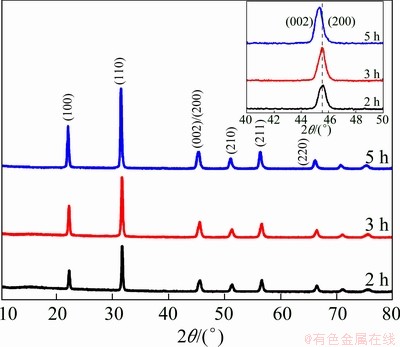
Fig. 1 XRD patterns of 0.98KNN-0.02LF ceramics sintered with different dwell time (the inset is the enlarged XRD patterns)
Figure 2 shows SEM images of surface microstructure for 0.98KNN-0.02LF ceramics sintered for different dwell time. As shown in Fig. 2(a), the grain sizes are distinctly smaller and more uniform compared with Figs. 2(b) and (c). The average grain size is about 1 μm for the sample sintered for the dwell time of 2 h and some distinct pores are found at grain boundaries. In Figs. 2(b) and (c), the samples show in general a bimodal grain size distribution. The small grain sizes are 1.0-2.0 μm and the coarse grain sizes are 3.0-5.0 μm for the sample sintered for the dwell time of 3 h, and the small grain sizes are 1.0-2.5 μm and the coarse grain sizes are 4.0-5.0 μm for the sample sintered for the dwell time of 5 h. Size increase is noted for the samples sintered for 3 h and 5 h. According to the phenomenological kinetic grain growth equation, with the increase in dwell time, grain size increases [19]. Moreover, it is clearly found that the pores are gradually decreased with increasing the dwell time. This result demonstrates that the dwell time has a great influence on the microstructure evolution of 0.98KNN-0.02LF ceramics.
Figure 3 shows the bulk density (BD) of 0.98KNN-0.02LF ceramics sintered for different dwell time with increasing the dwell time from 2 h to 5 h, the bulk density slightly increases from 4.26 g/cm3 to 4.29 g/cm3. This evolution agrees well with the LiTaO3-modified KNN ceramics that an increase of density is observed for dwell time of 10 h [20]. This is because these pores gradually decrease with increasing the dwell time. The average grain size and the density of this ceramic tend to increase with increasing the dwell time, probably because the grain growth is controlled by the boundary diffusion [21]. This indicates that the sintering process can enhance the diffusion and promote the densification of the sample.

Fig. 2 SEM images of surface microstructure for 0.98KNN-0.02LF ceramics sintered for different dwell time
Different microstructures may affect the electrical properties. Figure 4 provides the temperature dependent of dielectric permittivity (εr) and dielectric loss (tan δ) for 0.98KNN-0.02LF ceramics with different dwell time during sintering (measured at 10 kHz). It can be observed in Fig. 4(a) that the maximum dielectric permittivity decreases with increasing the dwell time, but the phase transition temperature is unmodified. These results agree well with the XRD patterns and indicate that there are no secondary impurities occurring. The decreased εr value can be attributed to the larger grain size with increasing the dwell time. It is well known that the piezoelectric and dielectric properties drop rapidly below a critical grain size and reach saturation at a larger grain size [22]. With increasing the grain size, the contribution from extrinsic effects, i.e. domain wall motion, will increase. It can be observed in Fig. 4(b) that the dielectric loss slightly decreases with increasing the dwell time when the temperature is below 400 °C; the dielectric loss increases rapidly with increasing the dwell time when the temperature is beyond 400 °C owing to the conductive loss. A similar behavior has also been observed in PZT-PCN systems [23]. According to Fig. 4, the dielectric permittivity maximum (εmax) of 0.98KNN- 0.02LF ceramics under the optimum dwell time has a value of approximately 2253 and tan δ is lower than 5% at a broad usage temperature range (100-400 °C). These results indicate its potential application in high temperature multilayer ceramics capacitor field.
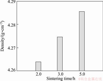
Fig. 3 Bulk density of 0.98KNN-0.02LF ceramics sintered for different dwell time

Fig. 4 Temperature dependence of dielectric permittivity (a) and dielectric loss (b) for 0.98KNN-0.02LF ceramics sintered for different dwell time (measured at 10 kHz)
Figure 5(a) shows the plot of the P―E loops of 0.98KNN- 0.02LF ceramics sintered for different dwell time, measured at room temperature and the frequency of 1 Hz. Saturated P―E hysteresis loops are demonstrated for all 0.98KNN-0.02LF ceramics in the present work. Generally, the existence of P―E hysteresis loops is considered an evidence that the material is ferroelectrics. In this study, the saturated P―E hysteresis loops confirm the ferroelectric nature of 0.98KNN-0.02LF ceramics. Figure 5(b) shows the 2Pr and 2Ec values of 0.98KNN-0.02LF ceramics sintered at different dwell time. The observed 2Pr value slightly decreases with increasing the dwell time, giving a maximum value of 34.51 μC/cm2 with a dwell time of 2 h. Different from 2Pr, the observed 2Ec value increases from 5.07 kV/mm to 6.08 kV/mm with the increase of dwell time (from 2 h to 5 h).
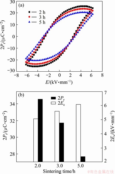
Fig. 5 P―E loops (a) and 2Pr and 2Ec values (b) of 0.98KNN-0.02LF ceramics sintered for different dwell time (measured at room temperature and frequency of 1 Hz)
4 Conclusions
1) The 0.98KNN-0.02LF lead-free ceramics sintered with different dwell time were prepared by the conventional solid-state sintering method. The phase structures in all samples are pure pseudo-cubic perovskite. The dwell time affects the microstructure and density of 0.98KNN-0.02LF ceramics. An increased bimodal grain size distribution and bulk density are observed for the samples prepared with increasing the dwell time.
2) The εmax and 2Pr values of 0.98KNN-0.02LF ceramics decrease, and the 2Ec value increases with increasing the dwell time. The optimum dwell time for 0.98KNN-0.02LF ceramics should be 2 h. Dielectric properties of 0.98KNN-0.02LF ceramics under the optimum dwell time are εr=2253 and tan δ<5% and ferroelectric properties are 2Pr=34.51 μC/cm2 and 2Ec=5.07 kV/mm.
References
[1] COWLEY R A, GVASALIYA S N, LUSHNIKOV S G, ROESSLI B, ROTARU G M. Relaxing with relaxors: A review of relaxor ferroelectrics [J]. Adv Mater, 2011, 60: 229-327.
[2] JIANG Y H, ZHAO Y, QIN B Q. Dielectric and piezoelectric properties of (1-x)(Bi1-yLiy)(Sc1-ySby)O3-xPbTiO3 high temperature relaxor ferroelectric ceramics [J]. Appl Phys Lett, 2008, 93: 022904.
[3] STRINGER C J, DONNELLY N J, SHROUT T R, RANDALL C A, ALBERTA E F, HACKENBERGER W S. Dielectric characteristics of perovskite-structured high-temperature relaxor ferroelectrics: The BiScO3-Pb(Mg1/3Nb2/3)O3-PbTiO3 ternary system [J]. J Am Ceram Soc, 2008, 91: 1781-1787.
[4] STRINGER C J, RANDALL C A. In situ TEM investigations of the high-temperature relaxor ferroelectric BiScO3-Pb(Mg1/3Nb2/3)O3- PbTiO3 ternary solid solution [J]. J Am Ceram Soc, 2007, 90: 1802-1807.
[5] GUO Y, KAKIMOTO K, OHSATO H. Structure and electrical properties of lead-free (Na0.5K0.5)NbO3-BaTiO3 ceramics [J]. Jpn J Appl Phys, 2004, 43: 6662-6666.
[6] GUO Y, KAKIMOTO K, OHSATO H. Dielectric and piezoelectric properties of lead-free (Na0.5K0.5)NbO3-SrTiO3 ceramics [J]. Solid State Commun, 2004, 129: 279-284.
[7] BOBNAR V, BERNARD J, KOSEC M. Relaxorlike dielectric properties and history-dependent effects in the lead-free K0.5Na0.5NbO3-SrTiO3 ceramic system [J]. Appl Phys Lett, 2004, 85: 994-996.
[8] KOSEC M, BOBNAR V, HROVAT M, BERNARD J, MALIC B, HOLC J. New lead-free relaxors based on the K0.5Na0.5NbO3- SrTiO3 solid solution [J]. J Mat Res, 2004, 19: 1849-1854.
[9] BOBNAR V, HOLC J, HROVAT M, KOSEC M. Relaxorlike dielectric dynamics in the lead-free K0.5Na0.5NbO3-SrZrO3 ceramic system [J]. J Appl Phys, 2007, 101: 074103.
[10] DU H L, ZHOU W C, LUO F, ZHU D M, QU S B, LI Y, PEI Z B. High Tm lead-free relaxor ferroelectrics with broad temperature usage range: 0.04BiScO3- 0.96(K0.5Na0.5)NbO3 [J]. J Appl Phys, 2008, 104: 044104.
[11] DU H L, ZHOU W C, LUO F, ZHU D M, QU S B, PEI Z B. Phase structure, dielectric properties, and relaxor behavior of (K0.5Na0.5)NbO3-(Ba0.5Sr0.5)TiO3 lead-free solid solution for high temperature applications [J]. J Appl Phys, 2009, 105: 124104.
[12] CHENG H L, DU H L, ZHOU W C, LUO F, ZHU D M. Effects of LaFeO3 additions on the dielectric and ferroelectric properties of (K0.5Na0.5)NbO3 ceramics [J]. J Inorganic Mater, 2012, 27: 1228-1232.
[13] ZHEN Y H, LI J F. Normal sintering of (K, Na)NbO3-based ceramics: Influence of sintering temperature on densification, microstructure and electrical properties [J]. J Am Ceram Soc, 2006, 89: 3669-3675.
[14] CHANG R C, CHU S Y, WONG Y P, HONG C S, UANG H H. The effects of sintering temperature on the properties of lead-free (Na0.5K0.5)NbO3-SrTiO3 ceramics [J]. J alloys Comp, 2008, 456: 308-312.
[15] ZHAO Y J, ZHAO Y Z, HUANG R X, LIU R E, ZHOU H P. Effect of sintering temperature on microstructure and electric properties of 0.95(K0.5Na0.5)NbO3-0.05Li(Nb0.5Sb0.5)O3 with copper oxide sintering aid [J]. J Am Ceram Soc, 2011, 94: 656-60.
[16] LI J F, ZHEN Y, ZHANG B P, ZHANG L M, WANG K. Normal sintering of (K, Na)NbO3-based lead-free piezoelectric ceramics [J]. Ceram Int, 2008, 34: 783-786.
[17] RUBIO-MARCOS F, OCHOA P, FERNANDEZ J F. Sintering and properties of lead free (K,Na,Li)(Nb,Ta,Sb)O3 ceramics [J]. J Eur Ceram Soc, 2007, 27: 4125-4129.
[18] LIU D J, DU H L, TANG F S. Effect of heating rate on the structure evolution of (K0.5Na0.5)NbO3-LiNbO3 lead-free piezoelectric ceramics [J]. J Electroceram, 2008, 20: 107-111.
[19] MCAFEE R J, NETTLESHIP I. A mesoscale description of microstructure evolution for the sintering of ceramics [J]. Acta Materialia, 2005, 53: 4305-4311.
[20] WANG Y, DAMJANOVIC D, KLEIN N, SETTER N. High- temperature instability of Li- and Ta-modified (K,Na)NbO3 piezoceramics [J]. J Am Ceram Soc, 2008, 91: 1962-1970.
[21] CHEN C Y, HU Y, LIN H L. A novel low temperature sintering process for PMnN-PZT ceramics [J]. Mater Chem Phys, 2006, 99: 26-29.
[22] CAO W, RANDALL C A. Grain size and domain size relations in bulk ceramic ferroelectric materials [J]. J Phys Chem Solids, 1996, 57: 1499-1505.
[23] ANURAK P, MUANGJAI U, ATHIPONG N. Dielectric and ferroelectric properties of 0.8PZT-0.2PCN ceramics under sintering conditions variation [J]. Current Applied Physics, 2009, 9: 1165-1169.
保温时间对0.98(K0.5Na0.5)NbO3-0.02LaFeO3陶瓷电性能的影响
程花蕾,周万城,杜红亮,罗 发,朱冬梅
西北工业大学 材料科学与工程学院,凝固技术国家重点实验室,西安 710072
摘 要:研究保温时间对0.98(K0.5Na0.5)NbO3-0.02LaFeO3(缩写为0.98KNN-0.02LF)无铅陶瓷相结构、显微组织、介电性能及铁电性能的影响。所有烧结样品均为纯的伪立方钙钛矿相,保温时间对相结构影响不大。随着保温时间的延长,样品的XRD衍射峰逐渐增强,并且向低角度移动。SEM观察结果显示,随着保温时间的延长,陶瓷样品的致密性提高,晶粒异常长大并出现孪晶结构。介电温谱表明,随着保温时间的延长,介电性能有所降低。电滞回线结果表明,2Pr随着保温时间的延长而增大的程度有所减小,而2Ec略有增加。在1150 °C烧结2 h得的到陶瓷的性能较优:εr=2253,tan δ<5%,2Pr=34.51 μC/cm2,2Ec=5.07 kV/mm。
关键词:铌酸钾钠;保温时间;介电性能;铁电性能;无铅陶瓷
(Edited by Hua YANG)
Foundation item: Project (CX201108) supported by the Doctorate Foundation of Northwestern Polytechnical University, China; Project (51072165) supported by the National Natural Science Foundation of China; Projects (KP200901, SKLSP201104) supported by the Fund of State Key Laboratory of Solidification Processing in NWPU, China
Corresponding author: Hua-lei CHENG; E-mail: hualeicheng@163.com
DOI: 10.1016/S1003-6326(13)62824-1

