
Structural and optical properties of tellurium films obtained by chemical vapor deposition(CVD)
MA Yu-tian(马玉天)1, 2,GONG Zhu-Qing(龚竹青)1, XU Wei-Hong(徐卫红)1, HUANG Jian(黄 坚)1
1. School of Metallurgical Science and Engineering, Central South University, Changsha 410083, China;
2. Jinchuan Group Ltd, Jinchang 737100, China
Received 18 July 2005; accepted 14 March 2006
Abstract: Tellurium thin films were prepared by the chemical vapor deposition method. The structure, surface morphology and optical properties of the Te thin films were analyzed by powder X-ray diffraction, scanning electron microscopy, FTIR transmission, UV/VIS/NIR transmission and reflectance. The results show that the films structural and optical properties are influenced by many factors such as film thickness, crystallite size and substrate temperature. The films as thick as 111-133 nm have high IR transmission across the full 8-13 μm band and highly blocking in the solar spectral region elsewhere, which indicates that Te films thickness in this region can be used as good solar radiation shields in radiative cooling devices.
Key words: tellurium thin film; chemical vapor deposition; solar radiation shields; radiative cooling
1 Introduction
Te thin films have been extensively used in various technological areas, especially in microelectronic devices such as gas sensor [1-3], optical information storage [4] and other applications [5-7]. All these applications are due to remarkable physical properties of Te such as low band-gap and transparency in the infrared region. In addition to above physical properties, Te films have another special characteristic, namely spectral selectivity, which can be used as shield in radiative cooling system [8-13].
Radiative cooling is the one among today,s challenges in materials science research. It occurs when a body gets cold by loosing energy through radiative processes. The phenomenon of radiative cooling uses the fact that the thermal energy emitted by a clear sky in the “atmospheric window region”(8-13 μm)[14] is much less than the thermal energy emitted by a blackbody at ground air temperature in this wavelength range. Hence, the surface on the earth facing the sky experiences an imbalance of outgoing and incoming thermal radiation and cools to below the ambient air temperature. While this concept can work well at night, assuming a relatively dry atmosphere, the solar energy input during the day, which is normally much greater than that radiated out, causes heating of the system. To prevent this, a shield is needed to cover the radiating surface in order to block solar radiation during the day as well as to prevent convective mixing in the cooled space. The ideal radiation shield would reflect solar radiation completely, but allow complete transmission in the “atmospheric- window” region. The polyethylene foils coated with thin films of Te that showed optical properties for cooling purpose[15].
In this study, Te thin films on microstructure and their optical properties were discussed in order to assess the possibility of Te thin films for radiative cooling system uses. Te thin films were chemically vapor deposited(CVD) on polyethylene foils[8, 9]. The structure, surface morphology and the optical properties of the films were studied by powder X-ray diffraction (XRD), scanning electron microscopy(SEM), FTIR spectrophotometer and UV/VIS/NIR spectrophotometer.
2 Experimental
2.1 Film preparation
Polymeric foils containing non-absorbing pigment offered the possibility to combine high reflectance of solar radiation with high transmittance in the atmospheric-window region. Other materials either absorb too strongly in window region or, as for high band gap semiconductors, are not feasible for large area application. Thin polyethylene foils are, at present, the only practical substrate for use as radiation shields. Polyethylene is non-absorbing ,except for characteristic absorption bands at 2.4, 3.4, 6.8 and 13.7 μm [8]. Extensive work using polyethylene foils and studying the effects of its transmittance properties in the atmospheric window have been done by AHMED et al [16] and DOBSON et al [8]. Thin commercial low-density polyethylene(LDPE) foils are selected as the substrate material due to its availability and constant optical properties, which are easy to obtain for the homemade samples. The FTIR transmission spectrum of LDPE foils (about 50 μm) used in this study is shown in Fig.1. Its characteristic absorption bands are 3.4, 3.5, 6.8, 7.3, 13.7 and 13.9 μm.
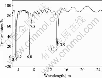
Fig.1 FTIR transmission spectra of bare low-density polyethylene foil
The LDPE foils was cut to 4 cm×5 cm in size, cleaned with detergent and rinsed well with water, immersed in a 10% KMnO4 solution for typically 24-48 h at room temperature and washed with water[8, 9]. Deposition of Te films according to the process was described in Refs.[9, 17].
A laboratory-scale experimental apparatus was used to generate H2Te and deposition of thin tellurium films onto polyethylene foil is illustrated in Fig.2. It consisted of ice bath, glass U cell, glass vessel, Pt anode, Te cathode, power supply and wash bottle.
The mixture gas (H2Te+N2) was led from the electrolysis cell into a glass vessel, the H2Te was decomposed as it passed through the glass vessel, leaving a film of Te on the polyethylene foil. The outlet of the glass vessel was led into a wash bottle of aqueous NaOH and CuSO4 solution to absorb any unreacted H2Te.
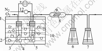
Fig.2 Diagram of laboratory-scale experimental apparatus: 1 Ice bath; 2 Ice and water; 3 Glass U cell; 4 Pt anode; 5 Te cathode; 6 Wash bottle(NaOH solution); 7 Wash bottle(CuSO4 solution); 8 Polyethylene foil; 9 Deposition vessel; 10 Pho- sphoric acid solution; 11 Power supply; 12 Flow meter
2.2 Test methods
The final thickness of the deposited Te films was calculated based on the mass change of the polyethylene before and after the film deposition, the film deposition speed was calculated from the thickness and deposition time.
Powder X-ray diffraction(XRD) was used to characterize the sample. The scan rate was 2?/min and covered the range between 10? and 80?.
The surface morphology of the films was observed with a JEOL JSM-5800 scanning electron microscope (SEM).
All FTIR spectra were recorded as direct (specular) transmission or reflection, while the UV/VIS/NIR spectra were obtained as diffuse transmission and reflectance. FTIR spectra were recorded on a NEXUS 470 spectrometer. The measurements were performed with normal incident light of 2.5-25 μm wavelength. Diffuse reflection and transmission spectroscopy measurements in the UV/VIS/NIR region were carried out on a Lambda 900 spectrophotometer equipped with an integrating sphere. Spectra were recorded at room temperature between 200 nm and 2000 nm, with a scanning rate of 400 nm/min.
3 Results and discussion
3.1 Optical characteristics of polyethylene substrate
The average transmission of bare LDPE foils in the atmospheric window is about 80% (Fig.1). As noted in the experimental section, we applied a modified KMnO4 pre-treatment of the polyethylene to improve adhesion of thicker films. The nature of this surface treatment has been discussed in detail elsewhere [9]. In short, the KMnO4 pretreatment forms a brown transparent MnO2 films, which does not affect the FTIR spectrum to any noticeable extent (Fig.3(a)).
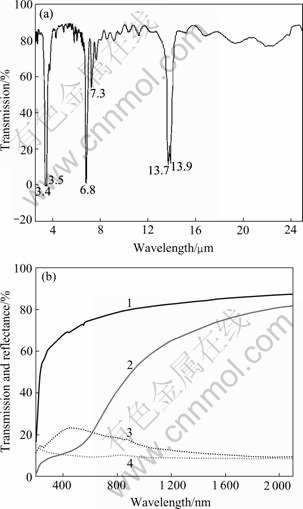
Fig.3 FTIR transmission spectra of Mn-O coated LDPE foil(a) and UV/VIS/NIR transmission and reflection spectra of bare and Mn-O coated LDPE foil(b): 1 Transmission of bare LDPE foil; 2 Transmission of Mn-O coated LDPE foil; 3 Reflection of Mn-O coated LDPE foil; 4 Reflection of bare LDPE foil.
Fig.3(b) shows that the brown Mn-O coated polyethylene film (curve 2) is much less transmitting than that of the bare polyethylene film (curve 1) in the visible region of the solar spectrum, mainly due to absorption and reflection. This characteristic is con- sidered advantageous for blocking the solar spectrum.
The UV/VIS/NIR reflectance spectra of those films are shown in Fig.3(b) (curves 3 and 4). The reflectance for Mn-O coated polyethylene film (curve 3) is higher compared with the reflectance for bare polyethylene film (curve 4) in the UV/VIS/NIR region.
3.2Growth of thin films
Fig.4 and Fig.5 show the relationship between film thickness and deposition time and temperature of substrate. As can be seen from Fig.4 and Fig.5, the thickness of the Te film rises with the increasing deposition time and substrate temperature. At the same deposition time, the increasing degree of the thickness of Te film at high substrate temperature was greater than that of Te film at low substrate temperature.
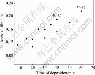
Fig.4 Relationship between film thickness and deposition time
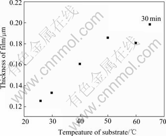
Fig.5 Relationship between film thickness and temperature of substrate
In general, the growth of good-quality tellurium thin films by the CVD technique proceeds at a suitable total gas flow rate in vessel and low temperature of substrate. The technique is ideally suited for product uniform tellurium films with thickness in the 0.03-0.3 μm range in most case. Deposition rate is dependent on the temperature of substrate and concentration of H2Te in the mixture gas. Higher deposition rates and higher film thickness are usually accompanied by powdery deposits and dis-homogenous thin films.
3.3 Structure properties of Te films
XRD patterns of Te films under different deposited times and substrate temperatures are presented in Fig.6. Table 1 lists the deposition condition and several characteristics of the films obtained from chemical vapor deposition method. As shown in Fig.6, the peaks at 2θ=27.65? and 38.39? due to diffraction of crystallo- graphic plane (011) and (102), respectively, become stronger with the increase of the deposition time in the thin film sample, which indicates that the phase structure of Te film is preferred oriented. As can be seen from Fig.6 and Table 1, the crystallite size and the thickness of the Te film rise with the increasing deposition time and substrate temperature. At the same deposition time, the crystallite size of Te at high substrate temperature is greater than that of Te at low substrate temperature and the increasing degree of the thickness of Te film under former condition faster than that of the latter. This attributes to the fact that the decompounded degree of H2Te rises with the increasing temperature[17].
Table 1 Deposition time, substrate temperature and several characteristics of Te film
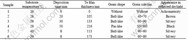
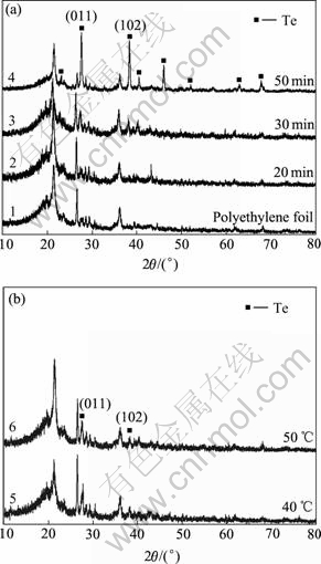
Fig.6 XRD patterns of polyethylene foil and Te films prepared under different conditions: (a) Substrate temperature 26 ℃; (b) Deposition time 8 min
Surface morphology is an important factor in determining the optical properties of semiconductor films. SEM image of polyethylene substrate (Fig.7(a)) and the same Te film as in Fig.6 are shown in Figs.7(b)-(f).
From Fig.7(a), it can be seen that the surface of polyethylene substrate is smooth. After deposition for 20 min, the smooth, homogeneous and compact Te film appear on the polyethylene substrate, the crystallite of Te has spherical microstructure, typical size is 40-70 nm (Fig.7(b)) and the color of Te film is brown appearance in reflected daylight (Table 1). In accordance with the increasing deposition time, the grain size of Te increases, the grain morphology remains spherical microstructure, which diameter is 60-90 nm, the silvery color appears and the texture of the Te film becomes more compact (Fig.7(c), Table 1). After deposition for more than 50 min, the grains have a pin-like shape (Fig.7(d)), which are the typical microstructure of powder Te. The Te film has dispersing texture, rough surface and black color (Table 1).
Figs.7(e) and (f) show the SEM micrographs of Te films obtained from deposited at different polyethylene substrate temperatures, respectively. With the increasing substrate temperature, the grain size of Te increases. However a lot of the grains on the film surface partially adhere to each other and the texture of the Te film becomes more compact. The typical needle shape microstructure of grains has lost, which may be attributed to the fact that the decompounded speed of H2Te is faster than that of the growth of crystalline Te.
3.4 Optical properties of Te films
The UV/VIS/NIR transmission and reflection spectra of polyethylene substrate 1 and the same Te films samples 2-6 as shown in Fig.6 are shown in Fig.8 and Fig.9, respectively. As can be seen from Fig.8(a), with the increase of the film thickness, from 105 nm to 216 nm, transmission decreases evidently in the UV/VIS/NIR region. The thicker Te film is less transmitting than that of the thin film in the UV/VIS/NIR region of the solar spectrum, and has an advantage for blocking the solar spectrum.
From Fig.8, it can be seen that the film has the same thickness (curves 2 and 5), but their transmissions are different in the UV/VIS/NIR region. This is due to the different surfaces of Te film shown in Figs.7(b) and (e). As can be seen from Fig.9, that the film of suitable thickness (samples 3 and 5), exhibits higher reflectance which, for the radiation with λ>800 nm, exceeds 45%. With increasing or decreasing Te film thickness (sample 4 or sample 2), the average reflectivity decreases. This phenomenon is explained through the film morphology. As the film thickness increases, the grain size increases too, as shown in Fig.7. The surface roughness increases with increasing grain size, which leads to the decrease of reflection[18]. Thinner film tends to difficultly obtain homogeneous films, which also decreases the reflection.
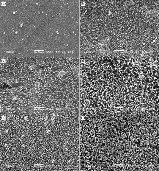
Fig.7 SEM photographs of polyethylene substrate and Te thin film prepared under different conditions: (a) Polyethylene substrate; (b) Substrate temperature 26 ℃, deposition time 20 min; (c) Substrate temperature 26 ℃, deposition time 30 min; (d) Substrate temperature 26 ℃, deposition time 50 min; (e) Substrate temperature 40 ℃, deposition time 8 min; (f) Substrate temperature 50 ℃, deposition time 8 min
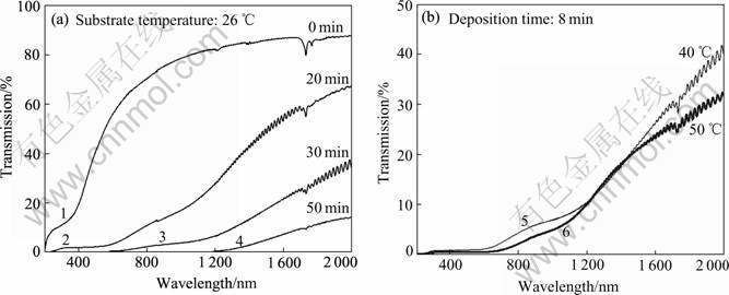
Fig.8 UV/VIS/NIR transmission spectra of polyethylene substrate and same Te film samples as shown in Fig.6
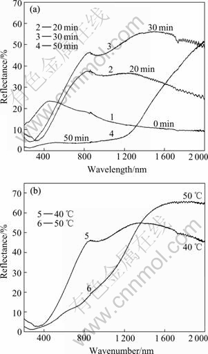
Fig.9 UV/VIS/NIR reflectance spectra of polyethylene substrate and same Te film samples as shown in Fig.6: (a) Substrate temperature 26 ℃; (b) Deposition time 8 min
Fig.10 shows the IR transmission spectra of the samples from Table 1.
From Fig.10, it can be seen that the Te film (samples 2-6) deposited on polyethylene exhibits an evident transmission which is greater than 60% for the radiation with the wavelength of 8-13 μm. The transmission decreases with increasing film thickness. Transmission of the Te film (curves 3 and 5) at 2.5 μm (which is close to the long wavelength edge of the solar spectrum) has dropped to 40% and 28%, respectively. These Te films (curves 3 and 5) do appear to possess the best properties for use in radiation shields.
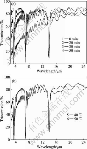
Fig.10 FTIR transmission spectra of polyethylene substrate and same Te film samples as shown in Fig.6: (a) Substrate temperature 26 ℃; (b) Deposition time 8 min
4 Conclusions
Te film was deposited on the low-density polyethylene foil by the CVD method. The analysed results show that the films structural and optical properties are influenced by many factors such as film thickness, crystallite size, substrate temperature. The optical properties analyses shown the films as thick as 111-133 nm have high IR transmission across the full 8-13 μm band, low transmission and high reflectance in the UV/VIS/NIR region. These characteristics are suitable for use as solar radiation shields in a radiative cooling system.
References
[1] TSIULYANU D, MARIAN S, LIESS H D, et al. Effect of annealing and temperature on the NO2 sensing properties of tellurium based films [J]. Sensors and Actuators B, 2004, 100(3): 380-386.
[2] SHASHWATI S, MUTHE K P, JOSHI N. Room temperature operating ammonia sensor based on tellurium thin films [J]. Sensors and Actuators B, 2004, 98(2-3): 154-159.
[3] TSIULYANU D, MARIAN S, MIRON V, et al. High sensitive tellurium based NO2 gas sensor [J]. Sensors and Actuators B, 2001, 73(1): 35-39.
[4] JOSEF P, DANA P, JAROSLAV B, et al. Nano-structured crystalline Te films by laser gas-phase pyrolysis of dimethyl tellurium [J]. Anal Appl Pyrolysis, 2004, 71(2): 739-746.
[5] LOZZI L, SANTUCCI S, DI NARDO S, et al. XPS, LEED and AFM investigation of the Si(100) surface after the deposition and annealing of tellurium thin films [J]. Surface Science, 1996, 352-354: 1027-1032.
[6] LOZZI L, DI NARDO S, PASSACANTANDO M, et al. Growth of Te thin films deposited at room temperature on the Si(100) 2×1 surface [J]. J of Electron Spectroscopy and Related Phen, 1995, 71(1): 39-45.
[7] LOZZI L, DI NARDO S, PASSACANTANDO M, et al. Electron spectroscopy investigation of Te thin films deposited at room temperature on Si(100) 2×1 [J]. Surface Science, 1995, 331-333(1): 569-574.
[8] DOBSON K D, HODESA G, MASTAIB Y. Thin semiconductor films for radiative cooling applications [J]. Solar Energy Materials & Solar Cells, 2003, 80(3): 283-296.
[9] ENGELHARD T, JONES E D, VINEY I, et al. Deposition of tellurium films by decomposition of electrochemically-generated H2Te: application to radiative cooling devices [J]. Thin Solid Films, 2000, 370(1-2): 101-105.
[10] NAIR P K, NAIR M T S, GARIA V M, et al. Semiconductor thin films by chemical bath deposition for solar energy related applications [J]. Solar Energy Materials and Solar Cells, 1998, 52(3-4): 313-344.
[11] TAKADA S. Research and development on passive cooling system [J]. Nuclear Engineering and Design, 2004, 233(1-3): 185-195.
[12] CAO B S, XUE Y Y, WOSIK J, et al. Hg-based HTS loop antenna used for the demonstration of a passive radiative cooler for spacecraft [J]. Physica C, 2000, 341-348(part 4): 2751-2752.
[13] TAZAWA M, JIN P, TANEMURA S. Thin film used to obtain a constant temperature lower than the ambient [J]. Thin Solid Films, 1996, 281-282(1-2): 232-234.
[14] NILSSON T M J, NIKLASSON G A . Radiative cooling during the day: simulations and experiments on pigmented polyethylene cover foils [J]. Solar Energy Materials & Solar Cells, 1995, 37(1): 93-118.
[15] DIATEZUA D M, THIRTY P A, DEREUX A, et al. Silicon oxynitride multilayers as spectrally selective material for passive radiative cooling applications [J]. Solar Energy Materials and Solar Cells, 1996, 40(3): 253-259.
[16] ALI A H H, SAITO H, TAHA I M S, et al. Effect of aging, thickness and color on both the radiative properties of polyethylene films and performance of the nocturnal cooling unit [J]. Energy Conversion and Management, 1998, 39(1-2): 87-93.
[17] ZHOU Ling-zhi. Handbook of Scattered Metals [M]. Changsha: Central South University Technology Press, 1983.
[18] POP I, NASCU C, IONESCU V, et al. Structural and optical properties of PbS thin films obtained by chemical deposition [J]. Thin Solid Films, 1997, 307(1-2): 240-244.
Foundation item: Project(50204001) supported by the National Natural Science Foundation of China
Corresponding author: MA Yu-tian; Tel: +86-731-8832548; +86-13077394490; E-mail: mayutian666@163.com
(Edited by LI Xiang-qun)

