Trans. Nonferrous Met. Soc. China 24(2014) 120-125
Preparation of YBa2Cu3O7-δ superconducting thick film on Ni-W tapes via electrophoretic deposition
Qing-wei LUO, Ying-nan LI, Feng-hua LI, Zhan-guo FAN
School of Materials and Metallurgy, Northeastern University, Shenyang 110819, China
Received 12 November 2012; accepted 12 March 2013
Abstract: The preparation of La0.4Sr0.6TiO3 (LSTO) buffer layer and YBa2Cu3O7-δ (YBCO) superconducting thick film by a low cost technology was studied. The crystal orientation of LSTO and YBCO films was detected by X-ray diffraction, the conductivity of LSTO film and superconductivity of YBCO coating were investigated by standard four-probe method. Excellent in-plane alignment, smooth and dense LSTO buffer layer was successfully prepared on textured Ni-W taps by metal organic deposition (MOD). YBCO thick film was fabricated by electrophoretic deposition (EPD). The effects of applied voltage and deposition time on the YBCO coatings properties were studied. The results show that the critical current density of the YBCO coating deposited under 138 V for 35 min was about 600 A/cm2 (0 T, 77 K).
Key words: conductive buffer layer; YBCO; superconducting thick film; electrophoretic deposition
1 Introduction
Due to their high transition temperature Tc, high critical current density Jc and upper magnetic field Hc2, the high temperature superconducting (HTS) materials hold great promise for wide commercial applications. Among the superconducting materials, YBCO is one of the greatest interests in the scientific community for its future technological application. Since the discovery of YBCO in the late 1980s, researchers have been looking for ways to produce affordable flexible conducting wire [1,2]. Numerous fabrication techniques of high temperature superconducting films had been studied extensively over the past few decades. Magnetron sputtering, metal organic chemical vapour deposition, pulsed laser deposition and physical vapour deposition are common approaches. However, the extensive applications were limited by the expensive apparatus, which makes them impractical for low cost application. Metal organic deposition (MOD) was more practical for application due to many advantages, such as low cost, precise controllability of the chemical stoichiometric and easy application to large substrates [3-5]. In particular, the electrophoretic deposition (EPD) technique has some outstanding features. It can be used to prepare ceramic materials into desired shapes and large scale, meanwhile, the thickness of film could be easily controlled. Moreover, it is high productivity and low cost [6-8].
SATO et al [9] investigated the effect of YBCO particle size reduction on crack formation, and the results showed that reduction in the particle size could effectively minimize deposit cracks and improve the YBCO film morphology. MgB2 superconducting films were prepared on stainless steel substrates via EPD approach, various deposition parameters were optimized, and the MgB2 films showed the superconducting transition in the range of 38.5-39 K [10]. DUSOULIER et al [11] deeply investigated the YBCO particles chemical instability in the process of YBCO via EPD process. Based on their results, pair particle potentials were calculated and different charging mechanisms of YBCO film surfaces in acetone were proposed. However, there was no related report about the preparation of YBCO film on Ni-W metal tapes via EPD process.
The YBCO film was fabricated on buffered Ni-W metal tapes by EPD process for the first time in this work. The aim of this work is to explore a low cost preparation technology for the coated conductor. First, La0.4Sr0.6TiO3 (LSTO) conductive buffer layer was prepared on the Ni-W substrate by MOD method, and then YBCO superconductive film was fabricated on the LSTO buffer layer/Ni-W composite structure via EPD approach.
2 Experimental
2.1 Pretreatment of metal tapes
Textured Ni-W tapes were cut into pieces with a size of 10 mm×5 mm×0.1 mm as metal substrates. As the compounds of some elements, such as oxygen, chlorine and carbon, may be adsorbed on the surface of the metal substrates, it is necessary to clean the metal substrates beforehand [12]. The substrates were cleaned by an ultrasonic apparatus in the solutions of 30% NaOH, 10% acetone and deionized water, respectively.
2.2 Preparation of LSTO films
In order to avoid the reaction or inter-diffusion, a buffer layer should be introduced between Ni-W substrate and YBCO superconductive layer. In this study, LSTO conductive buffer layer was prepared on the Ni-W substrate by MOD method. The preparation of the precursor solution was carried out under atmospheric conditions. In the process of preparing LSTO precursor solution, tetrabutyl titanate (C16H36O4Ti), lanthanum acetate (La(CH3COO)31.5H2O), and strontium acetate ((C2H3O2)2Sr) were used as raw materials, acetic acid and methanol were used as solvent. Spin coating method was used to coat LSTO thin film on the textured Ni-W substrate, and the coated LSTO thin film was annealed at 950 °C for 2 h under the mixture of argon and hydrogen (Ar-4%H2).
2.3 Preparation of YBCO powder
In this study, the YBCO powder was prepared by chemical solution-sinter method. A mixture of yttrium acetate, barium acetate and copper acetate was dissolved in propanoic acid so as to mix in atomic scale, and then the YBCO solution was prepared. The solution was dried into gel in a drying oven at 200 °C. The gel was sintered in a muffle furnace at 800 °C for 3 h, and the product was ground into YBCO fine powder with a mortar.
2.4 Electrophoretic deposition of YBCO film
The YBCO powder was suspended in an iodine-added acetone bath by ultrasonic dispersion. The suspension was colloidal. The quantities of YBCO powder, acetone and iodine were 0.15 g, 100 mL and 15 mg, respectively. The LSTO/Ni-W structure (10 mm × 5 mm × 0.1 mm) was used as cathode, and a Ni piece (50 mm × 30 mm × 0.5 mm) was used as counter electrode. The two electrodes were set into the suspension vertically with a separation of 20 mm, between which a voltage was applied. The wet coating was dried at 120 °C in an ambient atmosphere.
The coatings were subjected to sintering and annealing treatments in order to improve their mechanical properties and obtain the appropriate oxygen stoichiometry. KUANG et al [13] pointed out that the adhesion of YBCO film could be greatly improved by the post heat treatment. At the same time, it could depress the micro-cracks on the film and the weak links between the grain boundaries, which have an important influence on the superconducting property of YBCO film. In this study, the deposited YBCO film was heated in a high purity argon flow to 875 °C at 10 °C/min, held for 3 h, then cooled it to 450 °C at 1.5 °C/min, and held at 450 °C for 3 h in oxygen flow, and then cooled to room temperature.
In this work, the phase composition identification and crystal orientation identification were performed by X-ray diffraction (XRD) with a step size of 0.05° (power conditions: 35 kV, 25 mA, using the Cu Kα radiation). The surface morphologies of the films were examined by SSX-550 scanning electron microscopy (SEM). The YBCO powder reaction degree was tested by the Fourier Transform Infrared (FTIR) spectrometer (Nicolet 380). The grain size of YBCO powder was measured by Laser type particle size distribution analyzer (BT-9003H). The room temperature electric resistivity of LSTO buffer layer and superconductivity of YBCO film were measured by the standard four-probe method.
3 Results and discussion
3.1 Characterization of LSTO buffer layer
Crystal orientation analysis of the LSTO buffer layer was carried out by XRD. Figure 1 shows the XRD pattern of the LSTO conductive buffer layer after 950 °C heat treatment. In Fig. 1, the peak at 46.4° belongs to the LSTO buffer layer (200) orientation, and the peak at 51.8° belongs to Ni-W substrate. Only the LSTO (200) peak displays in the XRD pattern, no other orientation peaks appear, and the FWHM value of LSTO (200) peak is 0.41°. The buffer layer grains grow along the (l00) orientation. This observation is evidence that the buffer layer has a strong cube texture. The biaxial texture of Ni-W substrate is inherited by the LSTO buffer layer. Meanwhile, the film has good epitaxial quality.
Surface morphology of the LSTO film on Ni-W substrate was characterized using SEM. As can be seen from Fig. 2, the buffer layer is smooth, dense, crack- free and pinhole-free, which means the obtained LSTO film could effectively prevent the Ni diffusion from the Ni-W substrate. These results reveal that the obtained LSTO buffer layer is suitable for further deposition of other buffer layers or YBCO coating. The room temperature electric resistivity of LSTO buffer layer was measured by the standard four-probe method, and the result was 4.73×10⁻⁵ Ω・m.
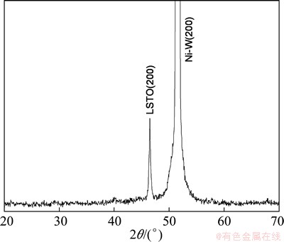
Fig. 1 XRD pattern of LSTO buffer film prepared by metal organic deposition
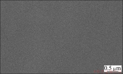
Fig. 2 SEM micrograph of LSTO thin film prepared by metal organic deposition
3.2 Analysis of YBCO powder
Figure 3 shows X-ray diffraction pattern of YBCO powder fabricated by chemical solution method. The diffraction pattern shows that the YBCO powder is single-phase YBa2Cu3O7-δ, and no other parasitic phases appear.
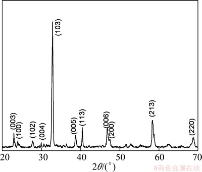
Fig. 3 XRD pattern of YBCO powder prepared by chemical solution-sinter method
For evaluating the completeness of reaction in the sintering process, the YBCO powder was measured by infrared spectroscopy KBr compression method. Figure 4 shows the IR spectra of YBCO powder. As shown in Fig. 4, the characteristic IR vibrating peaks of C―O―C, C―OH, ―CH2, ―C=O, C=C generated in the reaction process do not appear in the pattern. There are no other valence bond and functional groups vibrating peaks. That is to say, the YBCO powder crystallized fully after annealing process.
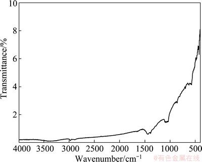
Fig. 4 IR spectrum of YBCO powder
Particle size has a prominent influence on controlling the cracking of the YBCO coating during drying and sintering. Reduction in particle size improves the morphology of the YBCO film, and it is a useful technique to minimize cracking of coatings [9]. To reduce the YBCO particle size, the powder was ground in the agate jar. The particle size distribution was measured by a Laser type particle size distribution analyzer (BT-9003H). Figure 5 shows the particle size distribution of YBCO powder synthesized by chemical solution-sinter technique for 5 h ball-milling. It shows that the average particle size is 1 μm.
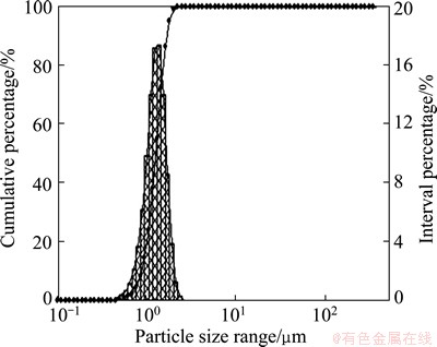
Fig. 5 Grain size distribution of powder ball-milled for 5 h
3.3 Effect of applied voltage on EPD
The directive voltage is an important parameter of electrophoretic deposition. The value of voltage affects the coated film thickness, the rate of deposition, the morphology of coated film, and the field emission property of cold cathode [14,15]. The YBCO electrophoretic deposition was performed under the condition of 128-138 V for 20 min. All the samples were sintered at 875 °C. Room temperature conductivity of the coatings is the criterion to infer superconducting performance indirectly. Figure 6 shows the room temperature resistance of YBCO film after heat treatment. From Fig. 6, it can be found that the room temperature resistance decreases along with the increase of applied voltage. The higher applied voltage is beneficial to the better electrical properties. However, higher applied voltage may cause turbulence in the suspension liquid, and the coating may be disturbed by flows in the surrounding medium, even during its deposition. In addition, particles can move so fast that they cannot have enough time to sit in their best positions to form a close-packed structure. Finally, because higher applied potential exerts more pressure on particle flux and movement, the applied field affects the deposition rate and the structure of the deposit.
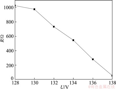
Fig. 6 Room temperature resistance of YBCO films prepared at different applied voltages
The film adhesion was characterized using cross cut test approach, which is the American Society for Testing Materials (ASTM) developed international standard for materials. The coating was divided into 25 square grids by a blade, the tape was spread on the grids and it was taken away quickly, then the shed situation of coating was obseved. There are 5 grades for adhesion intensity. The higher the ASTM grade is, the better the adhesion between coating and substrate is. Figure 7 shows the samples adhesion grades on Ni-W substrate. As shown in Fig. 7, coating adhesion become stronger gradually with the increase of applied voltage, which suggests that the higher electrophoretic voltage is beneficial to improving the coating adhesion intensity. Because of room temperature conductivity of YBCO coatings, 138 V is the best applied voltage.
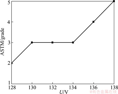
Fig. 7 YBCO film adhesion on substrate at different applied voltages
3.4 Effect of deposition time on EPD
Figure 8 shows the curve of YBCO deposition mass by EPD process at various deposition time. The EPD voltage was applied at 138 V. Figure 8 shows that in the EPD process, there is a linear relationship between deposition mass and time during the initial period (0-25 min). When the deposition time is longer than 25 min, the deposition mass attains a plateau at longer deposition time.
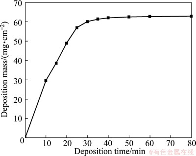
Fig. 8 Curve of YBCO deposition mass at different deposition time
Figure 9 shows the room temperature resistance of samples prepared by EPD at various deposition time. The curve clearly shows that the coating conductivity is linearly improved during the initial time (0-20 min). When the deposition time is prolonged to 25-40 min, the coating conductivity approaches to a constant. As time prolongs, the conductivity decreases very quickly.
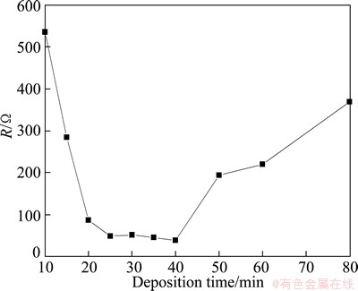
Fig. 9 Curve of room temperature resistance of YBCO films prepared at various deposition time
Figure 10 shows the surface micrograph of the YBCO film fabricated by EPD approach. The film is continuous, some pinholes appear on the surface, but no crack is found.
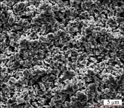
Fig. 10 SEM image of YBCO film prepared by EPD approach
Figure 11 shows the U-I curve of YBCO coating measured by the standard four-probe approach. According to the coating thickness and the sample size, the Jc of YBCO coating could be calculated. Based on calculations, the critical current density of the YBCO coating deposited for 35 min is about 600 A/cm2 (0 T, 77 K).
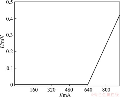
Fig. 11 U-I curve of YBCO coating measured by standard four-probe method
4 Conclusions
1) Excellent in-plane and biaxially textured LSTO buffer layer film was prepared on textured Ni-W tapes by MOD method. The room temperature electric resistivity of LSTO buffer layer was 4.73×10⁻⁵ Ω・m.
2) YBCO film was fabricated on LSTO conductive buffer layer by EPD approach. Effects of applied voltage and deposition time on the YBCO films properties were studied. The YBCO coating deposited under 138 V for 35 min exhibited a critical current value of 600 A/cm2 (self-field, 77 K).
3) MOD method combined with EPD approach could provide a new preparation technology for the coated conductor.
References
[1] GUO W, ZOU G S, CHAI X, WU A P, ZHENG M H, JIAO Y L, REN J L. The study of multiple thermal cycle of HTS YBCO bulk [J]. Physica C, 2012, 474: 25-28.
[2] MATIAS V, HAMMOND R H. YBCO superconductor wire based on IBAD-textured templates and RCE of YBCO: Process economics [J]. Physics Procedia, 2012, 36: 1440-1444.
[3] ZHAO P, ITO A, TU R, GOTO T. Fast epitaxial growth of a-axis and c-axis-oriented YBa2Cu3O7-δ films on (100) LaAlO3 substrate by laser chemical vapor deposition [J]. Applied Surface Science, 2011, 257(9): 4317-4320.
[4] JHA A K, KHARE N, PINTO R. Enhanced critical current density in YBa2Cu3O7-δ thin film deposited on La0.67Sr0.33MnO3 decorated SrTiO3 substrates [J]. Physica C, 2011, 471(22): 1154-1157.
[5] KNOTH K, HUHNE R, OSWALD S, MOLINA L, EIBL O, SCHULTZ L, HOLZAPFEL B. Homoepitaxial growth of MOD- YBCO thick films on evaporated and MOD templates [J]. Physica C, 2011, 471(21): 956-959.
[6] CAPRONI E, GOUVEA D, MUCCILLO R. Yttria-stabilized zirconia closed end tubes prepared by electrophoretic deposition [J]. Ceramics International, 2011, 37(1): 273-277.
[7] LI ZH M, QIAN SH Q, WANG W. Characterization and oxidation behavior of NiCoCrAlY coating fabricated by electrophoretic deposition and vacuum heat treatment [J]. Applied Surface Science, 2011, 257(10): 4616-4620.
[8] PANTGRAHI S, BHATTACHARJEE S, BESRA L, SINGH B P, SINGH S P. Electrophoretic deposition of doped ceria: Effect of solvents on deposition microstructure [J]. Journal of the European Ceramic Society, 2010, 30(5): 1097-1103.
[9] SATO N, KAWACHI M, NOTO K, YOSHIMOTO N, YOSHIZAWA M. Effect of particle size reduction on crack formation in electrophoretically deposited YBCO films [J]. Physica C, 2001, 357-360: 1019-22.
[10] KADAM M B, SINHA B B, KALUBARME R S, PAWAR S H. Transformation of MgB2 powder into superconducting film via electrophoretic deposition technique [J]. Journal of Alloys and Compounds, 2009, 478(1): 467-473.
[11] DUSOULIER L, CLOOTS R, VERTRUYEN B, MORENO R, MONTES B O, FERRARI B. YBa2Cu3O7-x dispersion in iodine acetone for electrophoretic deposition: Surface charging mechanism in a halogenated organic media [J]. Journal of the European Ceramic Society, 2011, 31(6): 1075-1086.
[12] SATHYAMURTHY S, SALAMA K. Chemical cleaning treatment of textured nickle for the deposition of epitaxial thin films [J]. Superconductor Science and Technology, 2004, 14: 643-645.
[13] KUANG X, CAROTENUTO G., NICOLAIS L. A review of ceramic sintering and suggestions on reducing sintering temperatures [J]. Advanced Performance Materials, 1997, 4: 257-274.
[14] WANG Y C, LEU I CH, HON M H. Kinetics of electrophoretic deposition for nanocrystalline zinc oxide coatings [J]. Journal of the American Ceramic Society, 2004, 87(1): 84-88.
[15] NEGISHI H, YANAGISHITA H, YOKOKAWA H. Electrophoretic deposition of solid oxide fuel cell material powders [J]. Proceedings of the Electrochemical Society on Electrophoretic Deposition: Fundamentals and Applications, 2002, 21: 214-219.
电泳沉积法在Ni-W基带上制备YBa2Cu3O7-δ超导厚膜
罗清威,李英楠,李凤华,樊占国
东北大学 材料与冶金学院,沈阳 110819
摘 要:研究La0.4Sr0.6TiO3 (LSTO) 缓冲层和YBa2Cu3O7-δ(YBCO)超导厚膜的低成本制备技术。采用X射线衍射分析LSTO和YBCO膜的晶体取向,利用标准四引线法分析LSTO薄膜的导电性能和YBCO厚膜的超导性能。首先采用金属有机沉积法(MOD)成功在Ni-W基带上制备取向较好、表面光滑致密的LSTO缓冲层;然后采用电泳沉积(EPD)技术制备YBCO超导厚膜。研究电泳沉积电压和沉积时间对YBCO涂层性能的影响。结果表明:138 V下电泳沉积35 min所制备的YBCO涂层,临界电流密度可达600 A/cm2 (0 T, 77 K)。
关键词:导电缓冲层;YBCO;超导厚膜;电泳沉积技术
(Edited by Chao WANG)
Foundation item: Project (N100602010) supported by the Fundamental Research Funds for the Central Universities of China
Corresponding author: Qing-wei LUO; Tel: +86-15524516939; E-mail: xiuhuanv1@126.com
DOI: 10.1016/S1003-6326(14)63036-3

