一种全频段GNSS应用的低噪声放大器
周仁杰1,马成炎1, 2, 3,项勇1,甘业兵1, 2, 3,叶甜春1
(1. 中国科学院微电子研究所,北京,100029;
2. 杭州中科微电子有限公司,浙江 杭州,310053;
3. 嘉兴联星微电子有限公司,浙江 嘉兴,314000)
摘要:设计一种满足全频段全球卫星导航系统(global navigation satellite system, GNSS)接收机应用要求的低噪声放大器(low noise amplifier, LNA)。为提高射频前端的集成度并降低成本,提出一种基于发射极电感负反馈结构宽带LNA的实现方法,并对电路结构、宽带输入阻抗匹配和噪声性能进行分析。电路采用0.18 μm SiGe BiCMOS工艺设计和实现。研究结果表明:在GNSS全频段范围(1 164~1 610 MHz)内,输入回损大于8.0 dB,输出回损大于8.9 dB,噪声系数低于1.30 dB,功率增益高于14.9 dB,输入三阶互调点为-5.8 dBm。芯片最低功耗为9.6 mW,面积约为600 μm×650 μm。
关键词:全球卫星导航系统(GNSS);全频段;低噪声放大器;SiGe BiCMOS;高集成度
中图分类号:TN433 文献标志码:A 文章编号:1672-7207(2014)07-2217-06
A low noise amplifier for full-band GNSS applications
ZHOU Renjie1, MA Chengyan1, 2, 3, XIONG Yong1, GAN Yebing1, 2, 3, YE Tianchun1
(1. Institute of Microelectronics, Chinese Academy of Science, Beijing 100029, China;
2. Hangzhou Zhongke Microelectronics Co. Ltd., Hangzhou 310053, China;
3. Jiaxing Lianxing Microelectronics Co. Ltd., Jiaxing 314000, China)
Abstract: A low noise amplifier (LNA) for full-band global navigation satellite system (GNSS) receivers was presented. To improve the integration of the RF front end and cut down the costs, an implementation method based on emitter-Inductor degenerated wide-band LNA was proposed. Then the architecture, wide-band input impedance matching and noise performance were analyzed. Based on 0.18 μm SiGe BiCMOS technology, the LNA was designed and implemented. The results show that the minimum input and output return losses are 8.0 dB and 8.9 dB respectively, the maximum noise figure is 1.30 dB, a minimum power gain of 14.9 dB and an IIP3 of -5.8 dBm are achieved in GNSS full-band from 1 164 MHz to 1 610 MHz. The minimum power consumption is 9.6 mW and the die area is about 600 μm×650 μm.
Key words: global navigation satellite system (GNSS); full-band; low noise amplifier (LNA); SiGe BiCMOS; high integration
随着GPS卫星导航系统的升级和完善以及包括俄罗斯GLONASS、中国北斗2号、欧洲Galileo等卫星导航系统的逐步建立健全,兼容多系统和多频段已经成为卫星导航接收机发展的主流方向[1]。现有的卫星导航信号载波频率分布在GPS L1频段和L2频段附近的多个频点,最低信号频率为1.164 GHz,最高为1.610 GHz。要实现对2个频段多个频点的支持,一般需要至少2个独立的LNA来分别放大不同频段的信号,这样在用于阻抗匹配的无源元件数目、芯片或者电路板面积、功耗以及成本方面都具有较大的开销。另外,由于卫星导航信号强度极弱,实现导航接收机的高接收灵敏度,射频前端的LNA自身必须具备极低的噪声系数和较高的功率增益以抑制后级电路模块的高噪声。因此,若能够用1个LNA来支持多频段乃至全频段应用,而同时保持低噪声系数和较高的功率增益,则能够带来集成度和成本等优势的显著提升。LNA实现多频段工作的解决方法一般有2种:(1) 进行经典的窄带放大器的设计,再通过切换匹配网络和谐振负载,使它工作在不同频段;(2) 将放大器设计成为1个宽带放大器,其带宽能够覆盖所有工作频段。这2种方法实现多频段LNA的研究较多[2-5]。相比较而言,采用第1种方法设计的窄带LNA一般具有较低的噪声系数以及较高的增益,但是由于其对于多频段的支持是建立在切换功能上,因此也就不具备同时工作在2个或者多个频段的能力。而第2种方法实现的宽带LNA,虽然一般来说噪声系数相对较大,但是无需进行频带切换,可以简化多频接收机系统设计,若能够针对具体应用对噪声系数进行优化,将是多频段接收机系统应用的理想选择。在此,本文作者在第2种方法基础上,分析并实现了面向全频段GNSS接收机系统应用要求的宽带LNA。对于射频微波集成电路,目前被广泛采用的是RF CMOS工艺以及SiGe BiCMOS工艺。前者具有CMOS工艺的高集成度和低成本优势,而后者具有优良的高频低噪声性能[6-7],在对性能要求较高的射频微波电路应用中是更合适的选择。因此,本文作者设计的面向全频段GNSS应用的单片集成LNA选择采用SiGe BiCMOS工艺设计和实现。
1 电路分析
1.1 结构分析
图1所示为发射极电感负反馈cascode LNA。由图1可见:共射级采用发射极电感负反馈结构,在保持低噪声系数的前提下,兼具输入匹配网络简单以及线性度优良的优点;共基级能够减小放大器共射级晶体管的高频密勒效应的影响、提高放大器的反向隔离度和增强稳定性。这种发射极电感负反馈共射共基(cascode)结构在无线收发机系统里被广泛应用[8]。
图2所示为全频段GNSS应用的LNA。由图2可见:在发射极电感负反馈cascode结构的基础上,LNA片内集成了输出阻抗匹配网络,仅需一个片外高Q电感,即可实现良好的输入输出阻抗匹配。由于发射极电感较小,可用封装键合线的寄生电感替代,以减小芯片面积。输出匹配网络由电感Lc,电容Cm,Cc和电阻R c组成。
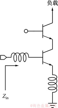
图1 发射极电感负反馈cascode LNA
Fig. 1 Emitter-inductor degenerated cascode LNA
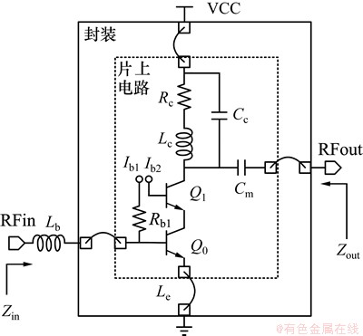
图2 全频段GNSS应用的LNA
Fig. 2 LNA for full-band GNSS application
1.2 输入匹配分析
输入匹配网络包括了输入节点的寄生电容包括焊盘的寄生电容、输入管的密勒等效电容和封装的寄生电容。输入匹配的实部由发射极电感提供,这个电感在本设计中采用封装键合线电感实现,以减小芯片面积。则输入阻抗为
 (1)
(1)
 (2)
(2)
其中:Lb和Le分别为基极和发射极电感; 和Cp分别为共射级的基极-发射极电容和输入节点寄生电容;
 为工作频率;
 为HBT管的单位电流增益特征频率;
 为源阻抗。若输入阻抗在中心频率处与源阻抗完全匹配,则由输入阻抗虚部完全抵消条件
 可以得到
可以得到
 (3)
(3)
若要在GNSS频带内有良好的输入阻抗匹配,则有
 <-10 dB (4)
设输入阻抗匹配带宽为W,则将式(1)代入式(4)可得
 (5)
(5)
从式(5)可知:输入阻抗与源阻抗完全匹配的条件下,输入匹配带宽W仅由Le和Lb决定,而这两者之和通常小于10 nH,这样BW将大于450 MHz,能够很好地满足GNSS全频段宽带输入阻抗匹配的要求。
1.3 噪声分析
对于输入匹配良好的HBT型LNA,其噪声系数为[9]

 (6)
(6)
其中:Rlb/Rs和rb/Rs分别为输入匹配电感与基极串联电阻的热噪声贡献; 为基极电流IB的散弹噪声贡献,最后一项是负载阻抗的噪声贡献,其余两项是集电极电流IC引入的噪声贡献。观察噪声系数表达式(1)可知:LNA的共射级应采用多指结构,以减其基极电阻的热噪声贡献,Lb宜采用片外高Q绕线电感以降低其等效串联电阻的噪声贡献。另外,噪声系数是
 的函数,且具有凹函数的特性,存在最优的使得噪声系数最优,而与HBT发射极电流密度直接相关[10],因此在实际设计中需要对HBT发射极电流密度进行优化以得到最优的噪声系数。
2 设计与实现
2.1 电路设计
本文设计的LNA,其共射级HBT晶体管的发射极面积为0.2 μm×2.0 μm。首先优化HBT的发射极电流密度,根据图3所示的仿真结果(为简便计,以下分析中仅考虑常温下的仿真和测试性能),在中心频率1.4 GHz附近,发射极电流密度Jc为100 μA/μm2左右时,最小噪声系数迅速降低到0.5 dB以下;在此发射极电流密度附近,功率增益与发射极电流密度正相关,为兼顾功率增益,选择发射极电流密度Jc约为200 μA/μm2,此时约为26 GHz。
为实现最优噪声匹配,需要对共射极HBT的并联个数N进行扫描,以使LNA的最优噪声源阻抗为50Ω。根据图4所示中心频率处的仿真结果,当N约为60时,LNA噪声系数达到最低,实现较好的噪声匹配。此时噪声系数约为1.08 dB,约为1.2 pF,而60个HBT单位晶体管一共消耗4.8 mA电流。
从式(2)计算可得发射极电感Le取值为0.3 nH,考虑焊盘和封装寄生电容的影响,实际取Le为0.5 nH,此电感由封装键合线电感实现,按照每根键合线电感约1 nH计算,需要2根并联才能满足输入阻抗匹配条件。输入节点总寄生电容 约为1.6 pF。由式(3)可知:输入匹配电感Lb为6 nH时能够得到较好的输入匹配。受输入节点寄生电容的影响,Lb实际取约5 nH。这样,由式(5)可得输入匹配带宽为W≈1 GHz。
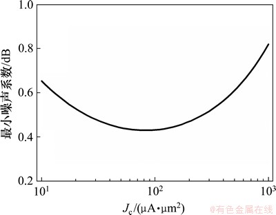
图3 HBT最小噪声系数与发射极电流密度Jc的关系
Fig. 3 Minimum noise figure of HBT with different emitter current densities Jc
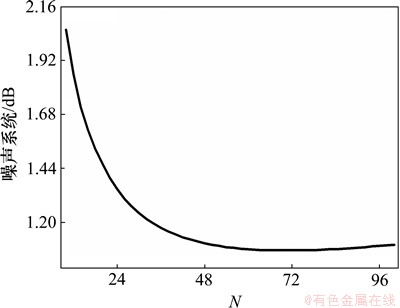
图4 LNA噪声系数与HBT晶体管数目N的关系
Fig. 4 Noise figure of LNA with different numbers of HBTs
共基级尺寸的选择主要考虑噪声系数和线性度的折中,尺寸太小会对噪声系数有明显的影响,而尺寸太大则会影响LNA的线性度,因此需要通过扫描分析进行确定,一般选择共射级尺寸的2/3到4/5比较适合,本设计中采用48个发射极面积为0.2 μm×2 μm的HBT单元管并联实现。
负载谐振网络中,片上螺旋电感Lc为5.2 nH,额外加入的8 Ω串联电阻Rc以降低Q和拓展带宽,另外负载端并联约2.7 pF的MiM电容,包括图2所示的Cc和Cm,与负载电感一起谐振在中心频率1.4 GHz附近,其功率增益1 dB带宽覆盖1.164~1.610 GHz。
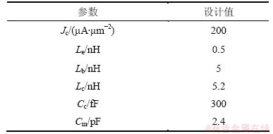
LNA采用电流镜偏置电路结构,偏置电流由片内基准电流源提供。LNA电路主要设计参数如表1所示。
表1 GNSS LNA设计参数
Table 1 Design parameters of GNSS LNAs
2.2 版图设计
本文设计的基于全频段GNSS应用的LNA,采用SiGe BiCMOS 0.18 μm工艺设计和实现,芯片显微照片如图5所示,芯片面积约为600 μm×650 μm。芯片设置SHDN控制端口,提供系统应用中的关断控制功能。按照2 000 V人体静电模型的要求,加入ESD保护电路。版图设计中,尽量减小射频地端口RF GND与模拟地GND之间的寄生电容,同时使射频输入RFin与射频输出RFout尽量远离,在芯片版图上处于对角位置,以减小寄生正反馈通路的环路增益,防止高频振荡。所有焊盘的底下设置接地的有源区,减小射频信号到衬底的损耗并增强LNA的反向隔离度。
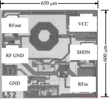
图5 LNA芯片显微照片
Fig. 5 Die photo of LNA
3 芯片测试与结果分析
芯片采用6管脚的小型DFN封装,以减小封装寄生对LNA性能的影响。测试电路采用基板介电常数较低的印刷电路板(PCB)以减小信号路径上的功率损耗。
使用Agilent E5062A型网络分析仪对LNA的S参数进行测量;使用Agilent N9020A型信号分析仪和N4000A型噪声源进行噪声系数的测量;使用Agilent E4438C型信号发生器和上述频谱分析仪进行输入三阶互调点IIP3的测量。
图6所示为LNA的S参数曲线。如图6(a)所示,S11在频率为1.164~1.610 GHz范围内小于-8.0 dB,并且在1.2~1.6 GHz范围内小于-10 dB。如图6(b)所示,S22在频率为1.164~1.610 GHz范围内小于-8.9 dB,并且在1.2~1.9 GHz范围内小于-10 dB。S11与S22的测量结果显示出优秀的宽带输入输出阻抗匹配性能。图 6(c)所示的S21曲线呈带通特性,在1.164 GHz处约为15.0 dB,在1.610 GHz处约为14.9 dB,最大值在约1.32 GHz处取到为16.0 dB,全频段功率增益较高,与16 dB设计目标较为接近,全频段增益不平坦度小于1.1 dB。图6(d)所示的S12在全频段范围内小于-30 dB,显示出优秀的反向隔离度。
图7所示为LNA的噪声系数测试结果。GNSS全频段范围内,噪声系数随频率递增,在1.164 GHz附近约为1.03 dB,在1.61 GHz处约为1.30 dB,显示出优异的宽带低噪声性能。
图8所示为LNA进行双音测试的输出信号频谱。输入信号频率分别为1.57 GHz和1.58 GHz,信号功率为-35 dBm。由图8可知:输出基频信号功率为-21.3 dBm(包含了约1 dB线损),输出三阶互调信号为-82.3 dBm。简单计算可知:输出三阶互调点OIP3为9.2 dBm,输入三阶互调点IIP3约为-5.8 dBm,显示出良好的线性度。
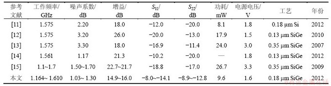
从测试结果看:本文提出的LNA具有宽带低噪声系数、高功率增益和高集成度的宽带输入输出匹配性能;在1.6 V电源电压时,包括偏置电路在内的总电流消耗仅为6 mA;与已发表文献中同类型LNA相比,具有明显的优势,如表2所示。
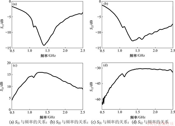
图6 GNSS LNA 的S参数测量值
Fig. 6 Measured S parameters of GNSS LNA
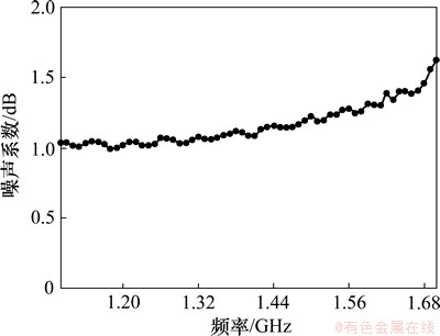
图7 噪声系数测量结果
Fig. 7 Measurement result of noise figure
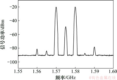
图8 LNA双音测试输出频谱
Fig. 8 Output of two-tone test of LNA
表2 GNSS LNA性能总结与比较
Table 2 Performance summary and comparison of GNSS LNAs
4 结论
(1) 提出了一种基于发射极电感负反馈结构宽带LNA的实现方法,并对电路结构、宽带输入阻抗匹配和噪声性能进行了分析,验证了这种方法的可行性。
(2)实现了基于0.18 μm SiGe BiCMOS工艺的GNSS全频段应用的宽带LNA。测试结果表明,LNA噪声系数在GNSS全频段范围内低于1.30 dB,功率增益高于14.9 dB,输入三阶互调点为-5.8 dBm。高集成度的输入输出阻抗匹配电路实现了较好的匹配性能,输入回损大于8.0 dB,输出回损大于8.9 dB。
参考文献:
[1] Ko J, Kim J, Cho S, et al. A 19-mW 2.6-mm2 L1/L2 dual-band CMOS GPS receiver[J]. IEEE Journal of Solid-State Circuits, 2005, 40(7): 1414-1425.
[2] Amor M B, Fakhfakh A, Mnif H, et al. Dual band CMOS LNA design with current reuse topology[J]. International Journal of Electronics, 2008, 95(3): 193-210.
[3] Dao V K, Choi B G, Park C S. Dual-band LNA for 2.4/5.2GHz applications[C]// Asia-Pacific Microwave Conference. Yokohama, 2006: 413-416.
[4] Chang W M, Cheng K H, Jou C F. 2.45 GHz/5.2 GHz switched dual-band CMOS LNA with 4 gain control modes[C]// Proceedings of Asia-Pacific Microwave Conference. Suzhou, 2005: 2-4.
[5] 武振宇, 马成炎, 叶甜春, 等. 一种可切换的双频段CMOS低噪声放大器[J]. 微电子学, 2010, 40(2): 217-221.
WU Zhenyu, MA Chengyan, YE Tianchun, et al. A switched dual-band CMOS LNA[J]. Chinese Journal of Microelectronics, 2010, 40(2): 217-221.
[6] Lee J, Cressler J D. Analysis and design of an ultra-wideband low-noise amplifier using resistive feedback in SiGe HBT technology[J]. IEEE Transactions on Microwave Theory and Techniques, 2006, 54(3): 1262-1268.
[7] Niu G. Noise in SiGe HBT RF technology: Physics, modeling, and circuit implications[J]. Proceedings of the IEEE, 2005, 93(9): 1583-1597.
[8] 池保勇, 余志平, 石秉学. CMOS射频集成电路分析与设计[M]. 北京: 清华大学出版社, 2006: 215-216.
CHI Baoyong, YU Zhiping, SHI Bingxue. Analysis and design of CMOS RF integrated circuits [M]. Beijing: Tsinghua University Press, 2006: 215-216.
[9] Sivonen P, Kangasmaa S, Parssinen A. Analysis of packaging effects and optimization in inductively degenerated common- emitter low-noise amplifiers[J]. IEEE Transactions on Microwave Theory and Techniques, 2003, 51(4): 1220-1226.
[10] Liang Q, Niu G, Cressler J D, et al. Geometry and bias current optimization for SiGe HBT cascode low-noise amplifiers[C]// IEEE Radio Frequency Integrated Circuits Symposium. Seattle, 2002: 407-410.
[11] 段炼, 黄伟, 马成炎, 等. ESD 保护低噪声放大器的分析与设计[J]. 微电子学, 2012, 42(5): 613-616.
DUAN Lian, HUANG Wei, MA Chengyan, et al. Analysis and design of low noise amplifier with ESD protection[J]. Chinese Journal of Microelectronics, 2012, 42(5): 613-616.
[12] Poh J C H, Cheng P, Thrivikraman T K, et al. High gain, high linearity, L-band SiGe low noise amplifier with fully-integrated matching network[C]// IEEE Topical Meeting on Silicon Monolithic Integrated Circuits in RF Systems. New Orleans, 2010: 69-72.
[13] Alvarado U, Rodriguez N, Mendizabal J, et al. A dual-gain ESD-protected LNA with integrated antenna sensor for a combined GALILEO and GPS front-end[C]// IEEE Topical Meeting on Silicon Monolithic Integrated Circuits in RF Systems. Long Beach, 2007: 99-102.
[14] Li J, Li W Y. A fully integrated LNA for COMPASS receiver in SiGe-BiCMOS technology[C]// IEEE MTT-S International Microwave Workshop Series on Millimeter Wave Wireless Technology and Applications (IMWS). Nanjing, 2012: 1-4.
[15] Hou X, Zhao Y, Li W, et al. Design of SiGe BiCMOS LNA with ESD protection for multi-band navigation receiver front-end[C]// IEEE Fifth International Conference on MEMS, NANO, and Smart Systems. Dubai, 2009: 93-96.
(编辑 杨幼平)
收稿日期:2013-07-15;修回日期:2013-10-10
基金项目:国家“核高基”重大专项(2009ZX01031-002-008);嘉兴市科技计划项目(2012BZ5006);嘉兴市南湖区科技计划项目(2011QG06)
通信作者:马成炎(1963-),男,江苏南通人,研究员,博士生导师,从事模拟射频集成电路和无线通信系统的设计和研究;电话:13670009918;E-mail: machengyan@casic.ac.cn

