J. Cent. South Univ. Technol. (2011) 18: 1572-1578
DOI: 10.1007/s11771-011-0874-4
1.0 V low voltage CMOS mixer based on voltage control load technique
WEI Bao-lin(韦保林)1, DAI Yu-jie(戴宇杰)2, ZHANG Xiao-xing(张小兴)2, L? Ying-jie(吕英杰)2
1. School of Information and Communication, Guilin University of Electronic Technology, Guilin 541004, China;
2. Institute of Microelectronics, Nankai University, Tianjin 300457, China
? Central South University Press and Springer-Verlag Berlin Heidelberg 2011
Abstract: A CMOS active mixer based on voltage control load technique which can operate at 1.0 V supply voltage was proposed, and its operation principle, noise and linearity analysis were also presented. Contrary to the conventional Gilbert-type mixer which is based on RF current-commutating, the load impedance in this proposed mixer is controlled by the LO signal, and it has only two stacked transistors at each branch which is suitable for low voltage applications. The mixer was designed and fabricated in 0.18 μm CMOS process for 2.4 GHz ISM band applications. With an input of 2.44 GHz RF signal and 2.442 GHz LO signal, the measurement specifications of the proposed mixer are: the conversion gain (GC) is 5.3 dB, the input-referred third-order intercept point (PIIP3) is 4.6 dBm, the input-referred 1 dB compression point (P1dB) is -7.4 dBm, and the single-sideband noise figure (NFSSB) is 21.7 dB.
Key words: CMOS active mixer; voltage control load technique; low voltage
1 Introduction
The essential goals in integrated circuit design are highly integrated, with low voltage, low power and so on. These characteristics are especially critical in mobile wireless communication systems due to the limitation of battery capacity. As the demand for multi-mode and multi-band communications with a single terminal is increased, achieving low-power consumption for the radio frequency (RF) circuits is the largest challenge in the scaled-down technologies. With reducing the scale of CMOS technologies, the key problem of analog and RF circuits integrated in sub-micron CMOS technologies comes from the continual reduction of supply voltages, hence resulting in poor performance [1-2]. Insufficient voltage headroom leads to the fact that not all circuit topologies are able to satisfy the required specifications, even some circuits cannot perform the function. Hence, research into low-voltage circuit topologies is important [1-5]. Mixer is the core component in both transmitter and receiver, and it needs to operate with low supply voltage and low power as other components.
The double balanced Gilbert-type mixer which is the most mature mixer architecture, is widely used as the down converter in CMOS super-heterodyne receiver, and it is composed of transconductance stage, switching stage, load stage and DC current tail. In this architecture, the stage of the transconductance transistor is switched on and off in each LO period. Due to large number of stacked transistors, this architecture cannot be used in CMOS sub-micron technologies which work with low supply voltage below 1.0 V [1]. Moreover, the main drawback of this architecture is transition needed for the transconductance stage in each period to go from off-mode to its saturation mode and vice versa, which degrades the linearity of mixer; therefore, this architecture achieves poor linearity [1-2].
To reduce the supply voltages, several low voltage mixer architectures have been investigated in Refs.[1-7], but they still have some drawbacks. Two folded mixer architectures were researched in Refs.[2,5], and they can operate at 1.0 V supply voltage. However, the main drawbacks of the folded mixer in Ref.[2] are: 1) The peak-to-peak amplitude of LO signal is lower than the supply voltages. 2) The circuit cannot be easily biased, in spite of the fact that the linearity and especially IIP3 performance of this circuit are dependent on proper biasing of transistor and switching section. 3) The switches are biased at non-zero drain current, which contributes more flicker noise to the output and increases the noise figure of the mixer. The main drawback of the folded mixer in Ref.[5] is that the linearity is very poor. Moreover, it consumes too much DC current, and the noise figure will be deteriorated severely if the RF signal declines.
A low voltage switched transconductor mixer was investigated in Ref.[6], which utilizes switches connected to the supply voltage. However, the source of transconductance stage is switched to the ground, switching DC voltage (Vdd,sw) in each LO period, which will generate considerable switching noise. Moreover, flicker noise (i.e. 1/f noise) of transconductance stage is mixed up, and the mixer needs two DC supply voltages (Vdd and Vdd,sw).
The low-voltage mixer in Ref.[7] is a folded- cascode, even harmonic mixer (FEHM). It can operate at 0.9 V low voltage, but the frequency-doubling technique must be employed in the local oscillator (LO) stage to produce a LO double-frequency signal, and two LC- tanks have to be adopted to reduce the voltage headroom and select the LO double-frequency signal, which would augment the chip area. Moreover, to improve the linearity and avoid gain degradation, an off-chip resistor-turning network which is composed of two large resistors has to be connected between the output of the current reuse circuit and the input of the buffer, and the IIP3 performance largely depends on the value of the resistor-turning network and the DC bias voltage of the RF stage and LO stage.
For 2.4-GHz ISM band applications, such as ZigBee, WLAN and Bluetooth, a low-voltage CMOS down- conversion mixer is proposed and implemented in this work.
2 Operation principle of voltage control load mixer
The single balanced version of the proposed mixer enhanced for low voltage applications in this study, based on variable load technology instead of RF current commutating, is shown in Fig.1. Transistors M3 and M4 operate in triode region, acting as the variable load [8], and their linear channel resistances are controlled by the LO signal:

 (1)
(1)
where  VTHP is the threshold voltage and μp is the mobility of charge carriers of PMOS transistors. W, L and Cox represent the width, length, and gate capacitance per unit area of the transistor. VBO and VB are the DC bias voltages. vRF and vLO are the RF and LO signals, respectively.
Transistors M1 and M2 act as the transconductance stage, and operate in saturation region. The single end output voltage of the circuit is
 (2)
(2)
where gmN is the transconductance of NMOS. In this design, the bias voltage and aspect ratio of transistors are selected to guarantee
 << 1 (3)
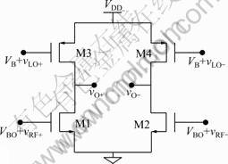
Fig.1 Single balanced version of proposed mixer based on voltage control load technique
Hence, by using Taylor series expansion, there is
 (4)
(4)
Therefore, Eqs.(1) and (2) can now be written as
 (5)
(5)
and

 (6)
(6)
The last term in Eq.(6) is proportional to vLOvRF, which can be used to perform mixing. The voltage conversion gain (GV) of the mixer is
 (7)
(7)
It can be seen from Eq.(7) that in order to improve the voltage conversion gain, βp (i.e. W/L) of the PMOS should be minimized, and VB and gmN should be maximized.
The mixer core proposed in Fig.1 has some shortcomings. Firstly, it can be seen from Eq.(6) that the output voltage contains the RF feedthrough term. Secondly, the LO feedthrough will be found in the output voltage if the channel length modulations of M1 and M2 are taken into account. To solve these problems, the double balance structure is proposed and shown in Fig.2. This double balance version can remove the RF term in the output voltage.
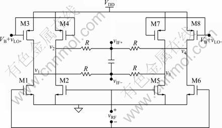
Fig.2 Double balanced version of proposed mixer based on voltage control load technique
In Fig.2, the drain voltages at M1, M2, M5 and M6, i.e. v1, v2, v3 and v4 are

 (8)
(8)
Hence

 (9)
(9)

(10)

(11)
It can be seen from Eq.(11) that the RF term in the output voltage is canceled. The voltage conversion gain (GV) of the double balanced version of the voltage control load mixer is identical with the single balanced version.
In the conventional Gilbert-type mixer, the RF voltage signal is introduced into the transductance stage, and is converted into RF current. The LO signal switches the RF current on and off, then the output current contains the mixing term and is converted into output voltage by using transistors or resistors as load. This kind of mixer usually has four stacked stages, so it is difficult to be used at low voltage such as sub 1.0 V. The proposed mixer in this work is based on voltage control load technique, and the load transistors (M3-M4 and M7-M8) can operate in triode region during the LO signal period, whose resistances (Ron) are controlled by the LO signal. It can easily operate at low supply voltage of 1.0 V, because it has only two stacked transistors at each branch.
3 Noise figure and linearity analysis
The proposed mixer is applied for low-IF down conversion, so thermal noise and flicker noise become the primary noise source. The noise factor of the mixer core in Fig.1 will be discussed, and the methodology and results can be readily extended to the double balanced version.
Let  represent the thermal noise current in the
drain due to the channel resistance. If the transistor operates in triode region, then there is [8-9]
 (12)
(12)
where k is the Boltzmann’s constant, T is the temperature, and Ron is the channel resistance.
For MOS transistor operating in saturation region, there is
 (13)
(13)
where the coefficient γ is derived to be equal to 2/3 for long channel transistors and may need to be replaced by a larger value for submicron MOSFETs. gm is the transconductance of transistor.
The flicker noise contribution from a MOSFET is
 (14)
(14)
where K is a process-dependent constant on the order of 10-25 V2F, and f is the frequency. As in Ref.[10], there is no switching in this mixer, so all noise contributions from M1, M2, M3 and M4 are directly propagated to the output. When referred to the RF input, from Eqs.(13) and (14), the noise term due to M1 and M2 can be calculated as [11-12]
 (15)
(15)
From Eqs.(12) and (14), the noise term due to M3 and M4, when referred to the RF input, can be calculated as

 (16)
(16)
The input-referred noise is given by

 (17)
(17)
Thus, the noise factor of the mixer core in Fig.1 is

 (18)
(18)
where RS is the source resistance. The corner frequency of the ?ick noise contribution from a MOSFET is [8]
 (19)
(19)
It can be seen from Eqs.(18) and (19) that one must choose enough MOSFET dimension to guarantee that the corner frequency of the ?icker noise is below the IF frequency, otherwise, the dominant noise source of the mixer would be the ?icker noise. By extending Eq.(18) to the double balanced version, a calculational noise figure of 11.8 dB is derived, in the case that the W/L of PMOS and NMOS are 160/0.2 and 100/0.5, respectively. Since Eq.(18) and its expansion do not include the RC network, the noise figure of Fig.2 will not be less than 11.8 dB, which can be confirmed by the simulation result of 18.2 dB.
Linearity is another important consideration in the mixer design. The linearity of the mixer in Fig.2 is determined by the linearity of the transconductance stage of the mixer and the load transistors. The linearity of transconductance has been discussed in Refs.[13-14]. Generally, transconductance linearity can be improved by increasing the gate overdrive voltage. As the basic operating principle for CMOS transistor suggests, CMOS has high linearity with low gain in linear region and low linearity with high gain in saturation region [15]. In the mixer proposed in this study, the load MOSFETs operate in the linear region, so they can help to improve the linearity but provide less gain. The MOSFETs of transductance stage operate in the saturation region, which helps to improve the gain but offer lower linearity. The linearity of the mixer core illustrated in Fig.1 will be discussed, and the methodology and results can be readily extended to the double balanced version.
The drain currents in M3 and M1 are

 (20)
(20)
 (21)
(21)
where  VTHN is the threshold voltage of M1 and M2, and μn is the mobility of charge carriers of NMOS transistors. Let
 (22)
(22)
 (23)
(23)
The current flow through M1 is equal to that of M3, so

 (24)
(24)
This gives
 (25)
(25)
By using Taylor series expansion, the expression of vo up to third-order terms can be gotten:
 (26)
(26)
where
 (27)
(27)
 (28)
(28)
 (29)
(29)
 (30)
(30)
 (31)
(31)
Hence,
 (32)
(32)
The input-referred third-order intercept point (IIP3) in voltage is
 (33)
(33)
It can be seen from Eqs.(32) and (33) that in order to increase the input-referred third-order intercept point (IIP3), B and VB0 should be maximized. Maximizing VB0 means improving the gate overdrive voltage of transductance stage. To improve B, one can aggrandize the W/L of the PMOS or reduce VB, but this will depress the voltage conversion gain (GV). Base on Eqs.(32) and (33), the calculational PIIP3 is 2.7 dBm under the same transistor size as mentioned previously, not considering the effect of RC network. As the RF feedthrough term in the output can be canceled by the RC network, the actual PIIP3 of the double balanced mixer will not be less than 2.7 dBm, which can be confirmed by the simulation result of 3.9 dBm.
4 Proposed mixer design and measurement results
The double balanced version of the proposed mixer which is depicted in Fig.2 has been fabricated in 0.18 μm CMOS process for 2.4 GHz ISM band applications. The chip micrograph is shown in Fig.3, and its active die size is 0.13 mm × 0.14 mm, not including the pads and ESDs. To avoid mismatches, all the transistors and metal connections in the circuit were placed as symmetrically as possible [16-17]. To reduce the flicker noise, the NMOS devices of transductance stage occupy large area, with the gate length of 0.5 μm and the width of 100 μm. The gate length of the PMOS is 0.2 μm and the width is 160 μm. All high frequency signals (i.e. RF and LO signal) are routed on the top or upper metal layer in order to reduce parasitics.
With a supply voltage of 1.0 V, the fabricated mixer probes. The RF port was driven by a 2.440 GHz RF was measured in 2.4 GHz ISM band with on-wafer RF signal, and the frequency of LO signal was 2.442 GHz. The DC bias voltages of VB0 and VB are 0.65 V and 0.25 V, respectively. It draws a DC current of 875 ?A from the supply at each branch. The RF signal powers have been corrected to compensate for the insertion loss of the passive balun, input matching circuit, cable and probe. The measurement results are shown in Figs.4, 5 and 6. Figure 4 illustrates the output spectrum of the two-tone test with two input RF frequencies of 2.440 1 GHz and 2.439 9 GHz, where Pout is the output power of the mixer. The measured input-referred third-order intercept point in power (PIIP3) is 4.6 dBm. The measured input-referred 1dB compression point (P1dB) is shown in Fig.5, indicating P1dB of -7.4 dBm. The measured result of PIIP3 is 1.7 dBm higher than the simulated result (3.9 dBm). This is because the parasitics resistance in the output contributes a little linearity.
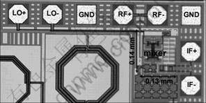
Fig.3 Micrograph of fabricated voltage control load mixer
The measured single-sideband noise figure (NFSSB) versus frequency is illustrated in Fig.6. It has NFSSB of 21.7 dB at the IF frequency of 2 MHz. Because four resistances in the RC filter contribute considerable noise to the output, the noise figure of the mixer is degraded. This noise figure is acceptable since the noise term caused by the mixer will be compressed by the LNA as for the noise figure of the front-end receiver. Because the actual parasitics resistance of the chip contributes more noise, measured result of NFSSB is 3.5 dB higher than the simulated result (18.2 dB).
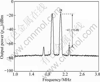
Fig.4 Output spectrum of two-tone test with input frequency spacing of 200 kHz
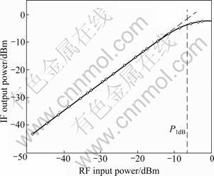
Fig.5 Measurement result of input-referred 1dB compression point (P1dB) of double balanced voltage control load mixer
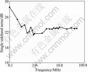
Fig.6 Measured result of single-sideband noise figure (NFSSB) versus frequency of double balanced voltage control load mixer
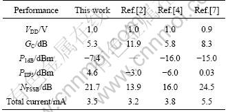
The main performance of the proposed mixer is summarized in Table 1, and compared with several published low voltage mixers. It can be seen that the linearity performance of this work is more competitive. High linearity performance is very important to the front-end receiver, because the linearity of mixer has great impact on the dynamic range of the receiver. This is a serious issue in low-voltage mixer design. Though the conversion gain (GC) of the mixers in Refs.[4, 7] is larger than that of this work, there are 4 or 5 inductors in these mixers which would augment their chip area. This point also becomes important for low-cost chip fabrication in more advanced CMOS process.
Table 1 Summary of measured results and performance comparison
5 Conclusions
1) To reduce the supply voltage, the active loads are accomplished using PMOSFETs, thus the number of stacked transistors are cut down, and the mixer can easily operate at 1.0 V supply voltage. The PMOSFETs can operate in triode region and can be controlled by the local signal, thus providing a voltage term proportional to vLOvRF at the output, which can perform the function of mixing.
2) The measurement results indicate the validity of the proposed mixer. Its linearity performance, the single sideband noise figure (NFSSB) and conversion gain (GC) performance are acceptable even under 1.0 V supply voltage. The proposed mixer is expected to operate at lower voltage in more advanced CMOS process due to circuit topology of two stacked transistors.
3) The voltage control load mixer is noninductive, which can help to reduce the chip area. It only occupies 0.13 mm × 0.14 mm chip area in 0.18 μm CMOS process, which is suitable for low-cost fabrication.
Acknowledgments
The authors would like to thank the Osaka University Global COE Program “Center for Electronic Devices Innovation” from the Ministry of Education, Culture, Sports, Science and Technology of Japan, for sponsoring this work. The authors would also like to thank Associate Professor Dr. MATSUOKA T and Dr. WANG J from Division of Electrical, Electronics and Information Engineering, Osaka University, for helping measurement.
References
[1] VAHIDFOR M B, SHOAEI O. A CMOS low voltage down- converter mixer for sub 1V applications [C]// IEEE Workshop on Microelectronics and Electron Devices. Boise: IEEE Press, 2006: 5-6.
[2] VIDOJKOVIC V, TANG J V D. A low-voltage folded-switching mixer in 0.18-μm CMOS [J]. IEEE Journal of Solid-State Circuits, 2005, 40(6): 1259-1264.
[3] HSIEH H H, LU L H. Designed of ultra-low-voltage RF front ends with complementary current-reused architectures [J]. IEEE Transactions on Microwave Theory and Techniques, 2007, 55(7): 1145-1158.
[4] CHEN C H, CHIANG P Y, CHRISTINA F J. A low voltage mixer with improved noise figure [J]. IEEE Microwave and Wireless Components Letters, 2009, 19(2): 92-94.
[5] WENG R M, WANG J C, WEI H C. A 1V 2.4 GHz down conversion folded mixer [C]// IEEE Asia Pacific Conference on Circuits and Systems. Singapore: IEEE Press, 2006: 1450-1452.
[6] KLUMPERINK E A M, LOUWSMA S M, WIENK G J M, NAUTA B. A CMOS switched transconductor mixer [J]. IEEE Journal of Solid-State Circuits, 2004, 39(8): 1231-1240.
[7] HUANG M F, KUO C J, LEE S Y. A 5.25-GHz CMOS folded-cascode even-harmonic mixer for low-voltage applications [J]. IEEE Transactions of Microwave Theory and Techniques, 2006, 54(2): 660-669.
[8] RAZAVI B. Design of analog CMOS integrated circuits [M]. New York: McGraw-Hill, 2001: 20-332.
[9] DARABI H, CHIU J. A noise cancellation technique in active RF-CMOS mixers [J]. IEEE Journal of Solid-State Circuits, 2005, 40(12): 2628-2632.
[10] LEUNG B. VLSI for wireless communication [M]. New Jersey: Prentice Hall, 2002: 151-165.
[11] LIU Lu, WANG Zhi-hua. Analysis and design of a low-voltage RF CMOS mixer [J]. IEEE Transactions on Circuits and Systems-II: Express Briefs, 2006, 53(3): 212-216.
[12] TERROVITIS M T, Meyer R G. Noise in current-commutating CMOS mixers [J]. IEEE Journal of Solid-State Circuits, 2006, 54(7): 2917-2924.
[13] TERROVITIS M T. Intermodulation distortion in current commutating CMOS mixers [J]. IEEE Journal of Solid-State Circuits, 2000, 35(10): 1461-1473.
[14] SOORAPANTH T, LEE T H. RF linearity of short-channel MOSFET’s [C]// 1st International Workshop on Design Mixed-Mode Integrate Circuits Application. Mexico: IEEE press, 1997: 81-84.
[15] NGUYEN T K, KRIZHANOVSKII V. A low-power RF direct- conversion receiver/transmitter for 2.4-GHz-band IEEE802.15.4 standard in 0.18-?m CMOS technology [J]. IEEE Transactions of Microwave Theory and Techniques, 2006, 54(12): 4062-4071.
[16] ROTELLA F, BHATTACHARYA B K, BLASCHKE V, MATLOUBIAN M, BROTMAN A, CHENG Y, DIVECHA R, HOWARD D, LAMPAERT K, MILIOZZI P, RACANELLI M, SINGH P, ZAMPARDI P J. A broad-band lumped element analytic model incorporating skin effect and substrate loss for inductors and inductor like components for silicon technology performance assessment and RFIC design [J]. IEEE Transactions on Electronic Devices, 2005, 52(7): 1429-1441.
[17] CHEUNG T S, LONG J. Shielded passive devices for silicon-based monolithic microwave and millimeter-wave integrated circuits [J]. IEEE Journal of Solid-state Circuits, 2006, 41(5): 1183-1200.
(Edited by YANG Bing)
Foundation item: Project(61166004) supported by the National Natural Science Foundation of China; Project(09ZCGHHZ00200) supported by the International Scientific and Technological Cooperation Program of Science and Technology Plan of Tianjin, China; Project(UF10028Y) supported by the Doctoral Scientific Research Foundation for Guilin University of Electronic Technology, China
Received date: 2010-12-08; Accepted date: 2011-04-05
Corresponding author: WEI Bao-lin, PhD; Tel: +86-773-2290203; E-mail: guilinwxb@163.com

