文章编号:1004-0609(2014)07-1817-06
石墨烯透明导电薄膜的合成与表征
王永祯,王 勇,刘志涛,蔡晓岚
(太原理工大学 材料科学与工程学院,太原 030024)
摘 要:以铜箔为基底采用化学气相沉积法(CVD)制备石墨烯透明导电薄膜,利用SEM、RAMAN、UV和四探针测试仪对产物微观形貌与结构、透光性和导电性能进行表征,讨论反应温度和氢气流量对石墨烯薄膜结构及性能的影响。结果表明:在一定范围内调节氢气流量均可得到石墨烯薄膜;当反应温度为1000 ℃时,制备的石墨烯缺陷和层数较少,透光性较高。随温度升高;石墨烯薄膜产生的缺陷和层数减少,石墨烯的薄层电阻随生长温度的升高呈线性下降趋势。石墨烯透明薄膜的微观结构与导电性相互关系的研究为其进一步应用于宽波长范围的窗口电极材料提供了理论基础。
关键词:石墨烯;透明导电薄膜;化学气相沉积;导电率
中图分类号:TQ127.1 文献标志码:A
Synthesis and characterization of graphene transparent conductive films
WANG Yong-zhen, WANG Yong, LIU Zhi-tao, CAI Xiao-lan
(College of Material Science and Engineering, Taiyuan University of Technology, Taiyuan 030024, China)
Abstract: Graphene transparent conductive films were prepared by CVD method using copper foils as substrates. The morphology and structure of sample were tested by SEM and Raman spectroscopy, and the optical and electrical properties were analyzed by UV spectrometer and Four probe instrument. The effects of temperature and hydrogen flow on the structure and properties of the treated graphene were studied. The results show that the high-quality few-layer graphene could be synthesized at 1000 ℃ with hydrogen flow in a moderate range. The sheet resistance of graphene indicates a linear downtrend with increasing the growth temperature. With increasing the temperature, the defect density and layers of graphene decrease, which results in an increase in the electrical conductivity. The study on the internal relations between structure and properties of graphene would promote its further application as a window electrode material with wider wavelength range.
Key words: graphene; transparent conductive film; chemical vapor deposition; electrical conductivity
具有高透光率和良好导电性的透明导电薄膜,被广泛应用在各种光电材料中[1-2]。2004年GEIM等[3]首次制备得到石墨烯,石墨烯独特的二维晶体结构赋予了其众多优异性能[4]。石墨烯的内部载流子密度高达1.0×1013 cm-2,室温下载流子迁移率为1.5×104 cm2/(V·s),具有较高的导电性;单层石墨烯的透光率为97.7%,透光性较高;此外,石墨烯还具有优异的机械柔韧性和化学稳定性。因此,石墨烯应用在光电器件领域具有较大潜力[5-6]。
化学气相沉积法能够制备大面积的高质量石墨烯,而且容易转移到各种目标基底,因此成为石墨烯透明导电薄膜的典型制备方法[7-9]。LEWIS等[10]以镍为基底制备得到石墨烯薄膜,经湿化学腐蚀转移至透明基底,探讨了其在有机光伏器件柔性电极方面的应用。卢向军等[11]和李兴鳌等[12]率先在铜箔上制得高质量的石墨烯薄膜,通过改进转移方法显著降低了石墨烯由于转移带来的缺陷。采用这种改进方法所制备的石墨烯更适合应用在透明导电电极上,为石墨烯基电子器件的制备奠定了基础。LEE等[13]以含氟高聚物作为转移介质将石墨烯薄膜转移到目标基底,转移时石墨烯上残留的含氟高聚物对石墨烯有掺杂作用,能够较大程度上降低其电阻,这类转移方法为石墨烯在透明电极上的应用提供了一个新思路。目前,石墨烯薄膜作为电极材料的研究主要集中在石墨烯薄膜制备上,而探索透明石墨烯导电薄膜结构与性能的关系对其在器件领域的应用至关重要。
本文作者通过化学气相沉积法(CVD)制备石墨烯透明导电薄膜,表征石墨烯薄膜结构及物理性能,探讨导电性、透光性与薄膜结构的内在关系,为石墨烯在透明电极材料领域的应用提供一定的理论基础。
1 实验
1.1 原料和仪器
主要原料如下:铜箔(厚度为25 μm,纯度为99.8%),莎阿法埃莎(天津)有限公司生产;甲烷、氢气、氩气等均为高纯度,太原市福江特种气体有限公司生产;丙酮、聚甲基丙烯酸甲酯(PMMA)、氯化铁等,均为分析纯,天津市光复科技发展有限公司生产;载玻片,海德创业(北京)生物科技有限公司生产;二氧化硅抛光片(氧化层厚度300 nm),浙江立晶光电科技有限公司生产。
主要仪器如下:InVia激光共焦显微拉曼光谱仪,英国雷尼绍公司生产;U-3900紫外-可见分光光度 计,日本HITACHI公司生产;RTS-9型双电测四探针测试仪,广州四探针科技有限公司生产。
1.2 石墨烯的合成
将铜箔裁剪成2 cm×2 cm大小,分别在丙酮和去离子水中超声清洗15 min,除去表面油污,然后将铜箔摆放在石英舟中置于反应室内的恒温区生长。典型的CVD生长过程如下:1) 将反应室抽至真空后填充氩气,如此反复操作3次;2) 在流量为300 mL/min的氢气气氛中升温至(1000±50) ℃时保温20 min,通过高温退火处理还原铜表面的氧化物;随后将温度调至生长所需温度,氢气流量调小至一定值(分别为30、60和90 mL/min),同时通入80 mL/min的氩气,继续恒温20 min,以避免氢气流量过大而引起的刻蚀;3) 保持其他条件不变,通入7 mL/min的甲烷,开始沉积石墨烯,生长时间为15 min;4) 停止通入甲烷,同时以10 ℃/min的降温速率开始冷却至室温,降温过程中其他气体流量不变。本研究中通过改变化学气相沉积(CVD)过程中生长温度和氢气流量等工艺条件,制得的9组石墨烯样品见表1。同时制备氢气流量为0和120 mL/min的样品作为对比样品。
表1 化学气相沉积法制备石墨烯薄膜的条件
Table 1 Preparation condition of graphene films by CVD

1.3 石墨烯的转移

图1 石墨烯薄膜的转移过程
Fig. 1 Transfer process of graphene films

图2 不同H2流量时铜箔表面的SEM像
Fig. 2 SEM images of copper surface by different H2 flow rates of 0 mL/min (a), 30 mL/min (b), 60 mL/min (c), 90 mL/min (d), and 120 mL/min (e)
生长出的石墨烯以铜箔作为基底,而铜箔存在一定的表面粗糙度,具有导电性和强烈的荧光背景,因此,石墨烯需转移至其他基底,如透明的载玻片、二氧化硅抛光片或柔性基底等。本实验中采用湿化学转移法[12],转移过程见图1。首先对生长后的铜箔表面旋涂PMMA溶液,在120 ℃下干燥10 min,PMMA层固化;然后浸入到0.5 mol/L FeCl3溶液中腐蚀铜基底(见图1(a)),由于铜箔正反两面均生长有石墨稀,为了避免反面石墨烯的干扰,浸润3~5 min后取出样品擦拭掉反面石墨烯;铜箔被完全腐蚀后,将PMMA/石墨烯移在去离子水中清洗干净(见图1(b));然后转移至目标基底,PMMA一侧朝上,晾干后用丙酮溶解去掉PMMA层,实现石墨烯在目标基底上的转移(见图1(c)~(d))。
2 结果与讨论
2.1 铜箔表面SEM分析
图2(a)所示为生长阶段通入的氢气流量为零时经过CVD过程后铜箔表面的SEM像。从图2(a)可以看到铜箔上附着大量细小的颗粒状无定形碳物质。这表明在常压体系没有氢气通入时,前驱体甲烷能够在铜的催化下裂解,但不能在铜箔表面生成石墨烯,只能生成无定形碳,氢气对碳的六元环结构的形成有催化作用。图2(b)、2(c)、2(d)所示分别为生长阶段通入的氢气流量分别为30、60和90 mL/min时铜箔表面的SEM像,从图中可以看出石墨烯完全覆盖铜箔表面,且跨越铜的晶界生长。图2(e)所示为生长阶段通入氢气流量为120 mL/min时铜箔表面的SEM像,其中深色区域为长有石墨烯的区域,浅色区域为铜箔基底。从图2(e)中可以看出石墨烯在铜箔表面呈不连续分布,这是由于较大的氢气流量使甲烷催化裂解速度降低,与此同时石墨烯的形核率降低、生长速度变慢。
2.2 拉曼光谱分析
图3所示为石墨烯薄膜的拉曼光谱。激光波长为514 nm,所有样品均转移至二氧化硅抛光片,避免铜基底的荧光背景干扰,每组样品随机取5点进行测试。由图3可见,所有的样品均出现了3个典型特征峰,D峰(约1350 cm-1处,sp2杂化碳蜂窝状结构的无序度指纹峰)、G峰(约1600 cm-1处,由sp2杂化C—C的面内伸缩振动引起)和2D峰(约2700 cm-1处,为二阶双共振过程,与石墨烯的层数有关),表明在不同的生长温度和氢气流量下均可制备得到石墨烯薄膜[14-15]。所有样品的D峰强度均很弱,相比G峰强度,ID/IG值为0.10~0.24,石墨烯结构缺陷较小。对每组样品随机测试5个点的拉曼数据几乎一致,表明制备的石墨烯薄膜质量较高且较均匀。通过2D峰与G峰的相对强度(I2D/IG)可以判断石墨烯的层数。由表2中各拉曼峰的统计结果可知,各样品的I2D/IG值均小于1,表明实验中制备得到的是3层以上的少层石墨烯[16-18]。尽管铜中碳溶量很低,但实验中甲烷气体所占比例相对较大,因此沉积得到少层石墨烯薄膜[19]。与单层或双层石墨烯相比,少层石墨烯具有一定的机械强度,有利于支撑薄膜的大面积生长,而且减弱了转移时造成的撕裂和折叠等对光电学性能的不利影响,能够较好地满足作为透明导电薄膜的应用要求[20-21];此外,层数的增加也弥补了单双层石墨烯中自由电子数量的不足。值得注意的是,石墨烯的透光率随层数的增加而降低,因此石墨烯的层数应控制在一定值。

图3 不同氢气流量下制备的石墨烯薄膜样品的拉曼光谱
Fig. 3 Raman spectra of graphene film sample prepared at various hydrogen flow rates
表2 不同氢气流量下石墨烯的拉曼峰统计结果
Table 2 Statistical results of Raman peak of grapheme

对比各样品2D峰的峰位及相对峰强I2D/IG(如表2),观察到样品b(30 mL/min,1000 ℃)、样品e(60 mL/min,1000 ℃)和样品h(90 mL/min,1000 ℃)3组样品的2D峰均位于2710 cm-1左右,且I2D/IG值较高,表明生长温度为1000 ℃时制备得到的石墨烯薄膜的层数最少,约5层左右。生长过程中氢气流在一定范围时,生长温度是影响石墨烯薄膜生长的重要因素,1000 ℃有利于生长层数较少的高质量石墨烯。
2.3 透光率测试
图4所示为石墨烯薄膜在可见光范围内的透光率测试结果,波长范围为400~1000 nm,所有样品均转移至透明的载玻片上,测试前通过裸露的载玻片进行校准,避免载玻片对样品透光率的准确性产生干扰。由图可见,1000 ℃时的3组样品的透光率较高,透光率约为86%,石墨烯的层数为(5±1)层[12, 22],与拉曼数据的分析结果一致。随着氢气流量的增大(如90 mL/min),制备的石墨烯薄膜的透光性较好,且受温度的影响较小,原因可能是氢气流量较大时,甲烷气体所占比例相对减小,沉积的石墨烯薄膜的层数较少,因此透光率较高[23]。生长温度为1000 ℃时制备的石墨烯薄膜在较宽的波长范围内均有较高的透光率,适合应用于波长较宽的光电器件的窗口电极材料。

图4 石墨烯薄膜的可见光透光率(插图为波长550 nm时的透光率)
Fig. 4 Visible light transmittance of graphene film
2.4 薄膜电阻测试
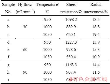
表3所列为石墨烯薄膜的平均薄层电阻值和径向不均匀度,每组样品随机取20个点测试,然后求其平均值。由表3中数据可以看出,石墨烯薄膜的电阻值均随生长温度的升高而降低,而与氢气流量无关。相对较低的温度不利于石墨烯薄膜的生长,往往产生较多的缺陷结构(与表2中ID/IG值一致),导致薄层电阻值增大;随着生长温度升高,制备的石墨烯缺陷减少,薄层电阻值相应降低[24]。石墨烯的层数也是影响其电阻值的因素之一[22, 25]。生长温度高有利于制备导电性良好的石墨烯薄膜。此外,由表中数据可知,所有样品的径向不均匀度均小于20%,在电阻测试误差允许范围内,说明制备的石墨烯薄膜均匀性较好。
表3 石墨烯薄膜的电阻值测试结果
Table 3 Test results of resistance of graphene films
3 结论
1) 以铜箔为基底,采用CVD法在(1000±50)℃的温度范围内均制得了高质量的少层石墨烯透明导电薄膜。研究表明,氢气流量在30~90 mL/min 范围内,1000 ℃时制备的石墨烯薄膜缺陷少,层数较少,因此透光性也较强。
2) 石墨烯的薄层电阻随生长温度的升高呈线性下降趋势。生长温度越高,制备的石墨烯的导电性越好。这主要是由于较低温度下制备的石墨烯缺陷多,随生长温度的提高,石墨烯的缺陷减小,薄层电阻降低。
REFERENCES
[1] 邹志宇, 戴博雅, 刘忠范. 石墨烯的化学气相沉积生长与过程工程学研究[J]. 中国科学: 化学, 2013, 3(1): 1-17.
ZOU Zhi-yu, DAI Bo-ya, LIU Zhong-fan. CVD process engineering for designed growth of graphene[J]. Scientia Sinica Chimica, 2013, 3(1): 1-17.
[2] LEE Young-bin, AHN Jong-hyun. Graphene-based transparent conductive films[J]. Nano, 2013, 8(3): 1330001.
[3] NOVOSELOV K S, GEIM A K, MOROZOV S. Electric field effect in atomically thin carbon films[J]. Science, 2004, 306(5696): 666-669.
[4] ZHU Yan-wu, MURALI S, CAI Wei-wei, LI Xue-song, SUK Ji-won, POTTS J R, RUOFF R S. Graphene and graphene oxide: synthesis, properties, and applications[J]. Advanced Materials, 2010, 22(35): 3906-3924.
[5] WASSEI J K, KANER R B. Graphene, a promising transparent conductor[J]. Materials Today, 2010, 13(3): 52-59.
[6] PANG Shu-ping, HERNANDEZ Y, FENG Xin-liang,  K. Graphene as transparent electrode material for organic electronics[J]. Advanced Materials, 2011, 23(25): 2779-2795.
[7] 王永祯, 王 艳, 韩 非, 蔡晓岚. 还原热处理对石墨烯薄膜导电性的影响[J]. 新型炭材料, 2012, 27(4): 266-270.
WANG Yong-zhen, WANG Yan, HAN Fei, CAI Xiao-lan. The effect of heat treatment on the electrical conductivity of highly conducting graphene films[J]. New Carbon Materials, 2012, 27(4): 266-270.
[8] KOBAYASHI T, BANDO M, KIMURA N, SHIMIZU K, KADONO K, UMEZU N, MIYAHARA K, HAYAZAKI S, NAGAI S, MIZUGUCHI Y, MURAKAMI Y, HOBARA D. Production of a 100 m-long high-quality graphene transparent conductive film by roll-to-roll chemical vapor deposition and transfer process[J]. Applied Physics Letters, 2013, 102(2): 023112.
[9] 任文才, 高力波, 马来鹏, 成会明. 石墨烯的化学气相沉积法制备[J]. 新型炭材料, 2011, 26(1): 71-80.
REN Wen-cai, GAO Li-bo, MA Lai-peng, CHENG Hui-ming. Preparation of graphene by chemical vapor deposition[J]. New Carbon Materials, 2011, 26(1): 71-80.
[10] HU Jie, WANG Li na, MA Jia hua, HUANG Hao. Preparation and photocatalytic performance of LaBO3(B=Ni, Mn, Fe)/graphene composite thin film[J]. Transactions Nonferrous Metals Society of China, 2012, 22(1): 2517-2522.
[11] 卢向军, 窦 辉, 杨苏东, 郝 亮, 张 方, 张校刚. 自支撑石墨烯,聚苯胺纳米纤维薄膜的制备及其电化学电容行为[J]. 物理化学学报, 2011, 27(10): 2333-2339.
LU Xiang-jun, DOU Hui, YANG Hui-dong, HAO Liang, ZHANG Xiao-gang. Fabrication and electrochemical capacitive behavior of freestanding graphene/polyaniline nanofibre film[J]. Chinese Journal of Physical Chemistry, 2011, 27(10): 2333-2339.
[12] 李兴鳌, 王博琳, 刘忠儒. 石墨烯的制备, 表征与特性研究进展[J]. 材料导报, 2012, 26(1): 61-65.
LI Xin-gao, WANG Bo-lin, LIU Zhong-ru. Research progress in preparation, characterization and properties of graphene[J]. Materials Review, 2012, 26(1): 61-65.
[13] LEE Wi-hyoung, SUK Ji-won, LEE Jong-ho, HAO Yu-feng, PARK Jae-sung, YANG Jae-won, HA Hyung-wook, MURALI S, CHOU H, AKINWANDE D, KIM K S, RUOFF R S. Simultaneous transfer and doping of CVD-Grown graphene by fluoropolymer for transparent conductive films on plastic[J]. ACS nano, 2012, 6(2): 1284-1290.
[14] DRESSELHAUS M S, JORIO A, HOFMANN M, DRESSELHAUS G, SAITO R. Perspectives on carbon nanotubes and graphene Raman spectroscopy[J]. Nano Lett, 2010, 10(3): 751-758.
[15] 黄宛真, 杨 倩, 叶晓丹, 孔凡志. 石墨烯层数的表征[J]. 材料导报, 2012, 26(7): 26-30.
HUANG Wan-zhen, YANG Qian, YE Xiao-dan, KONG Fan-zhi. Characterization of graphene layers[J]. Materials Review, 2012, 26(7): 26-30.
[16] 陈炳地, 彭成信, 崔 征. 高性能锂离子电池负极材料CoO/石墨烯纳米复合结构的超声法制备[J]. 中国有色金属学报, 2010, 26(8): 2073-2086.
CHEN Bing-di, PENG Cheng-xin, CUI Zheng. Ultrasonic synthesis of CoO/graphene nanohybrids as high performance anode materials for lithium-ion batteries[J]. Chinese Journal of Nonferrous Metals, 2010, 26(8): 2073-2086.
[17] HAO Yu-feng, WANG Ying-ying, WANG Lei, NI Zhen-hua, WANG Zi-qian, WANG Rui, KO Chee-keong, SHEN Ze-xiang, THONG J T L. Probing layer number and stacking order of few-layer graphene by raman spectroscopy[J]. Small, 2010, 6(2): 195-200.
[18] LIAO Chun-da, LU Yi-ying, TAMALAMPUDI S R, CHENG Hung-chieh, CHEN Yit-tsong. Chemical vapor deposition synthesis and raman spectroscopic characterization of large-area graphene sheets[J]. The Journal of Physical Chemistry A, 2013, 117(39): 9454-9461.
[19] ROBERTSON A W, WARNER J H. Hexagonal single crystal domains of few-layer graphene on copper foils[J]. Nano Letters, 2011, 11(3): 1182-1189.
[20] 陈 旭, 何大平, 木士春. 掺氮石墨烯研究[J]. 化学进展[J]. 2011, 11(3): 1182-1189.
CHEN Xu, HE Da-ping, MU Shi-chun. Nitrogen doped graphene research[J]. Progress in Chemistry, 2011, 11(3): 1182-1189
[21] WANG Wen-rong, CHEN Liang, WANG Zhe, WANG Yu-chen, LI Tie, WANG Yue-lin. Weak localization in few-layer graphene grown on copper foils by chemical vapor deposition[J]. Carbon, 2012, 50(14): 5242-5246.
[22] LEE Seung-hyun, LEE Kyung-hoon, LIU Chang-hua, ZHONG Zhao-hui. Homogeneous bilayer graphene film based flexible transparent conductor[J]. Nanoscale, 2012, 4(2): 639-644.
[23] LIU Wei, LI Hong, XU Chuan, KHATAMI Y, BANERJEE K. Synthesis of high-quality monolayer and bilayer graphene on copper using chemical vapor deposition[J]. Carbon, 2011, 49(13): 4122-4130.
[24] REGMI M, CHISHOLM M F, ERES G. The effect of growth parameters on the intrinsic properties of large-area single layer graphene grown by chemical vapor deposition on Cu[J]. Carbon, 2011, 50(1): 134-141.
[25] KASRY A, KURODA M A, MARTYNA G J, TULEVSKI G S, BOL A A. Chemical doping of large-area stacked graphene films for use as transparent, conducting electrodes[J]. ACS Nano, 2010, 4(7): 3839-3844.
(编辑 龙怀中)
基金项目:国家自然科学基金资助项目(51372160,51172152);山西省留学基金资助项目(2013-028)
收稿日期:2014-03-06;修订日期:2014-07-20
通信作者:王永祯,副教授,博士;电话:0351-6010768;E-mail:wangyongzhen@tyut.edu.cn

