文章编号:1004-0609(2007)03-0368-05
射频反应磁控溅射制备氮化铜薄膜
肖剑荣1, 2,徐 慧1,刘小良1,李燕峰1,张鹏华2,简献忠3
(1. 中南大学 物理科学与技术学院,长沙 410083;
2. 中南大学 材料科学与工程学院,长沙 410083;
3. 上海理工大学 电气工程学院,上海 200093)
摘 要:使用射频反应磁控溅射法,在不同的射频功率和气体流量比下制备了氮化铜薄膜,并用X射线衍射仪和原子力显微镜对薄膜的结构进行表征。研究结果表明:薄膜呈现择优生长规律,由低气体流量比的Cu3N(111)晶面转向高分压的(100)面;薄膜的光学带隙在1.44~1.69 eV之间,电阻率在60~5.6×10⁵ Ω?m之间,二者都随气体流量比的增大而增大。
关键词:氮化铜薄膜;晶体结构;光学带隙;电阻率
中图分类号:O484 文献标识码:A
Copper nitride thin films prepared by radio frequency magnetron sputtering
XIAO Jian-rong1, 2, XU Hui1, LIU Xiao-liang1, LI Yan-feng1, ZHANG Peng-hua2, JIAN Xian-zhong3
(1. School of Physics Science and Technology, Central South University, Changsha 410083, China;
2. School of Material Science and Engineering, Central South University, Changsha 410083, China;
3. School of Electric and Engineering, University of Shanghai Science and Technology, ShangHai 200093, China)
Abstract: Copper nitride (Cu3N) thin films were deposited by reactive radio frequency magnetron sputtering under different discharge powers and gas flow ratios. The structures of films were characterized by atomic force microscopy (AFM) and X-ray diffraction spectra (XRD). The properties of films were analyzed by UV-VIS spectra and four-probe method. The results show that the films’ growth prefers (111) direction at low nitrogen press and (100) direction at high nitrogen pressure. The optical band gap of the films ranges from 1.44 to 1.69 eV, the resistivity ranges from 60 to 5.6×10⁵Ω?m, and they both increase with the increase of nitrogen pressure.
Key words: copper nitride thin films; crystal structure; optical band gap; resistivity
氮化铜(Cu3N)为棕黑色晶体,具有反三氧化铼晶格结构,晶格常数为0.381 5 nm[1-2],属亚稳共价化合物,在较低的温度(250~470 ℃)下分解为N2和Cu[3-4],这与其他铜的化合物性质很不相同[5-6]。在Cu3N晶体中,由于铜原子并不是很好地占据晶格(111)面的紧密位置,因此在其晶体结构中留下了许多空隙。如果其他原子(如过渡金属Cu和Pb等)进入该空隙位,它的电学和光学性质就会发生显著变化[7-9]。长期以来,人们认为铜与氮气都是反应活性小的物质,所以,研究者开始以为氮化铜只能用复分解反应制得。Zachwieja等[10]在室温下,利用Cu(NH3)4(NO3)2与液氨混和并加入铜,制得长约为1 mm的氮化铜单晶纳米线。近年来,Cu3N可作为一种应用于高速集成电路和光存储器件的新型候选材料而备受人们的关注,相继利用Ar离子[11]和激光电子束[12]在Cu3N薄膜上刻蚀出铜点。这些特性有可能被用作光数据存储[13]。Borsa等[14]利用外延制备的Cu3N/γ′-Fe4N双层膜平整光滑,证实该膜可用作集成电路的隧道层材料。理论上,Cu3N薄膜光学带隙约为0.9 eV [1, 3, 7],而实验值却在1.1~1.9 eV之间[15-16]。Maruyama等[17]发现Cu3N薄膜随着晶格常数的变化可实现绝缘体向导体的过渡。而Yang等[18]发现Cu3N在5.5 GPa左右的压力下可实现半导体向导体的转变。可见,Cu3N结构特殊,物理性质十分独特,且具有广阔的应用前景,但人们对其物理性能变化原因、晶体结构变化与制备工艺之间的关系等不太清楚。在此,本文作者采用射频反应磁控溅射法制备Cu3N薄膜,并以气体流量比为主要研究参数,分析流量比对Cu3N薄膜晶体结构影响,以探讨其电学、光学性质与结构之间的内在联系。
1 实验
实验中采用铜(99.99%)为靶材,氮气(99.999%)和氩气(99.999%)的混合气作为工作气体,玻璃片作为基片。基片在放入真空室前,分别依次浸泡于丙酮、酒精溶液中,用超声波清洗20 min,然后,用去离子水冲洗,再用烘箱烘干。每次沉积时,真空室的本底压强低于2.0 mPa,溅射前,先在Ar气氛中预溅射10 min(流量20 cm3/min),对靶面和基底进行清理,再通入氮气,沉积氮化铜薄膜样品。在溅射过程中,氮气和氩气的总流量固定在50 cm3/min (氮气和氩气流量分别使用不同的质量流量控制仪控制),溅射气压为5.0 Pa。实验中以气体流量比和射频功率为研究参量,当射频功率为200 W不变时,气体流量比分别取0.10, 0.25、0.50、0.75和1.00进行实验。当气体流量比保持在0.75不变时,射频功率分别取100、200和300 W。在沉积过程中,基片温度控制在120 ℃不变,沉积时间均为10 min。
薄膜的表面形貌用Solver P47型原子力显微镜(AFM)进行表征。用D/max 250型全自动X射线衍射仪(XRD)对Cu3N薄膜的晶体结构进行表征。用TU-1800型紫外可见光谱仪(UV-VIS)研究薄膜的光吸收特性,求得薄膜的光学带隙。用SZT-90型四探针测试仪测得薄膜的电阻率。
2 结果和分析
2.1 薄膜的表面形貌
所制备的薄膜中含有Cu3N和Cu两相,因此,薄膜的颜色与这两相密切相关。由于使用的靶材是纯铜,随着Cu3N含量的增多,薄膜能够从Cu相的黄色一直变化到Cu3N相的棕黑色。图1所示为是沉积功率为200 W、气体流量比为0.75时沉积的Cu3N薄膜1.1 μm×1.1 μm的AFM三维表面形貌图,可见,薄膜表面平紧、致密,薄膜的最高峰值为15.447 nm,粗糙度为1.443 nm,均方根粗糙度为1.754 nm。
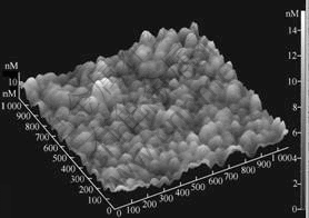
图1 Cu3N薄膜的AFM表面形貌
Fig.1 AFM image of Cu3N thin films
2.2 薄膜结构分析
在不同流量比下(沉积功率为200 W)制备的薄膜样品的XRD谱见图2。可见:随着气体流量比的增大,Cu3N薄膜在23.32?处的(100)晶面衍射峰逐渐加强,而41.05?处的(111)晶面衍射峰逐渐减弱。这说明薄膜在不同流量比下择优生长:在低的流量比下Cu3N薄膜择优(111)晶面生长,而在较高的流量比下沿(100)晶面择优生长。在b和c中出现Cu3N薄膜微弱的(110)衍射峰,而在a和d中几乎没有(110)衍射峰,说明只有在适当的r下(110)晶面才会生长。可见,气体流量比会影响Cu3N薄膜各晶面择优生长的取向[18]。其原因是:在低流量比下,主要是被吸附氮原子插入铜原子的晶格形成Cu―N键而成膜,薄膜是按照与Cu(111)晶面一致的晶向生长Cu3N(111)面;在高流量比下,有足够的氮原子与铜在靶表面或基片表面结合成CuN,这时,薄膜按照晶面自由能最低优先生长的原则生长Cu3N(100)面。图3所示为流量比是0.75时,不同沉积功率下制备的Cu3N薄膜XRD谱。可见,衍射谱中23.32?处的(100)和47.74?处(200)衍射峰随着功率的增加迅速增高,而其他衍射则没有变化。因此,沉积功率只能影响薄膜内的晶化程度,而对膜内晶体的生长取向没有影响。
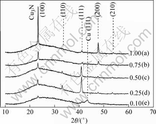
图2 不同流量比下Cu3N薄膜的XRD谱
Fig.2 XRD patterns of Cu3N thin films deposited at different gas flow ratios
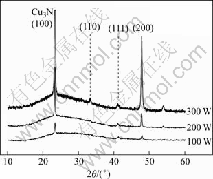
图3 不同沉积功率下Cu3N薄膜的XRD谱
Fig.3 XRD patterns of Cu3N thin films deposited at different discharge powers
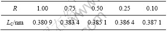
由不同流量比下Cu3N薄膜的XRD谱,通过仪器计算得到薄膜的晶格常数,结果见表1。其中:LC为晶格常数,R为流量比。可见,实验所得的Cu3N薄膜的晶格常数最小值为0.380 9 nm,最大值仅为0.387 1 nm,随着流量比的减小而增大。同时发现,它们比其他研究者报道的实验值(0.386 8 nm左右)偏小[17], 这可能是由于样品的制备方法和测试仪器的不同所引起。在Maruyama等的报道中[17],Cu3N薄膜的晶格常数在0.386 8 nm以上时,它为导体,而在0.386 8 nm以下时则为半导体。
表1 不同流量比下制备Cu3N薄膜的晶格常数
Table 1 Lattice constants (LC) of Cu3N films deposited at different gas flow ratios (R)
2.3 薄膜的光学和电学性质
图4所示为典型的Cu3N薄膜UV-VIS透射图谱(沉积功率为200 W,流量比0.75)。其中,Eg为光学带隙能。可见,Cu3N薄膜在蓝光区和紫光区有强吸收特性,而在红外区有很好的透射率。根据所得薄膜透射光谱曲线,按照从透射光谱计算薄膜光学常数的方法,可获得弱吸收、中等吸收和强吸收区薄膜的吸收系数α,再由Tauc方程[19]外推得到薄膜的光学带隙能Eg。

式中 α、hv和A分别为光学吸收系数、光子能量和常数。这样可得该条件下薄膜样品的光学带隙为1.58 eV,如图4中插图所示。利用该方法可得到不同沉积条件下薄膜的光学带隙,图5中曲线1是薄膜的光学带隙与气体流量比的关系曲线。显然,光学带隙随气体流量比的增大而增大。
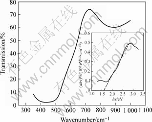
图4 典型的Cu3N薄膜UV-VIS透射谱
Fig.4 Typical transmission spectra of Cu3N films
在Cu3N晶体中,由于铜的s能带与氮原子p能带交叠,形成满带,所以,纯Cu3N晶体是绝缘体。但是,Cu3N晶体特殊的反三氧化铼晶格结构,很容易被别的原子填充到Cu3N晶格的中心空位而引起晶体本身电学性质改变,可使Cu3N晶体实现从绝缘体向半导体甚至导体转变。利用四探针方法在室温下对样品的电阻率进行测量,测量结果见图5中曲线2。可见,Cu3N薄膜样品的电阻率随气体流量比的增加而增大,呈指数规律变化,能够从导体的60 Ω?m变化到半导体的400 Ω?m左右,然后增大至近5.6×10⁵ Ω?m。所制备的薄膜样品中,仅有1个样品的电阻率处于导体范围(10-8~102 Ω?m),其余样品的电阻率均处于半导体范围(103~107 Ω?m)。在较低的气体流量比下,薄膜的电阻率增长较慢,变化不大,当气体流量比较大时,电阻率则增长很快。这一结果与其他研究者所得结果类似[13]。
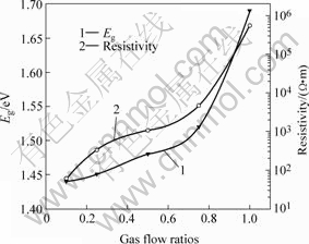
图5 薄膜光学带隙和薄膜电阻率与流量比的关系
Fig.5 Relationships among optical band gap, resistivity and gas flow ratios
比较图5中曲线1和2可见,两者变化趋势十分相似,都随着流量比的增大而增大,不过电阻率按指数规律变化,增加较快。产生这种现象的原因是:当流量比较低时,较多的被溅射出来的单质铜原子还来不及在靶表面和基底上与氮反应,就沉积在基片上。因此,Cu3N薄膜主要靠被吸附氮原子插入铜原子的晶格形成Cu―N键而形成。这时,由于在薄膜表面有相当一部分的铜原子没有与氮结合成键,所以,Cu3N晶格的中心空位仍含有较多的铜原子。这些填隙的Cu原子提供了弱局域化电子,而这些弱局域化电子相对以共价键结合的Cu3N晶格上的电子来说,具有非局域性,它们的存在能改变膜内电子态密度分布,此时薄膜完全具有半导体甚至导体的特性,即电阻率小,光学带隙小。当流量比很高时,高浓度的氮氛围使得有足量的氮原子与铜原子反应形成Cu―N键,导致薄膜中不再存在填隙的铜原子,形成电阻率相对较高甚至接近绝缘体的Cu3N薄膜,其光学带隙较大。
3 结论
1) 薄膜表面平整致密,颗粒均匀,平均粗糙度为1.443 nm。
2) 流量比影响Cu3N薄膜择优生长取向:随着流量比的增大,由低流量比下主要生长的Cu3N(111)晶面逐渐转向高流量比下生长的Cu3N(100)晶面。薄膜的晶格常数在0.380 9~0.387 1 nm之间, 且随着流量比的增大而减小。
3) 制备的薄膜样品光学带隙在1.44~1.69 eV之间,电阻率在60~5.6×10⁵ Ω?m之间,二者都随着流量比的增大而增大。
致谢
感谢中南大学物理科学与技术学院杨兵初教授、罗成林老师在样品制备与测试时给予的大力支持和帮助。
REFERENCES
[1] WEN Yu, ZHAO Jing-geng, JIN Chang-qing. Simultaneous softening of Cu3N phonon modes along the T2 line under pressure: A first-principles calculation [J]. Phys Rev B, 2005, 72: 214116-214124.
[2] Wang J, Chen J T, Yuan X M, et al. Copper nitride (Cu3N) thin films deposited by RF magnetron sputtering [J]. J Crystal Growth, 2006, 286:407-412.
[3] Moreno-Armenta M G, Martínez-Ruiz A. Ab initio total energy calculations of copper nitride: the effect of lattice parameters and Cu content in the electronic properties [J]. Solid State Sciences, 2004, 6: 9-14.
[4] Maruyama T, Morishita T. Copper nitride and tin nitride thin films for write-once optical recording media [J]. Appl Phys Lett, 1996,69 (7): 890-891.
[5] 易振华,易茂中,冉丽萍,杨 琳. 添加钛对炭/炭复合材料渗铜的影响[J]. 中国有色金属学报,2006, 16(7): 1214-1218.
YI Zhen-hua, YI Mao-zhong, RAN Li-ping, YANG Lin. Influence of adding Ti on molten copper infiltration into C/C composites[J]. The Chinese Journal of Nonferrous Metals, 2006, 16(7): 1214-1218.
[6] 关鲁雄,李家元,王 婷,等. 掺杂铜和钒的纳米二氧化钛的光催化性能[J]. 中南大学学报:自然科学版,2006, 37(4): 731-736.
GUAN Lu-xiong, LI Jia-yuan, WANG Ting, et al. Photocatalysis of nanometer-sized TiO2 particles doped with Cu2+ and V5+[J]. J Cent South Univ (Science and Technology), 2006, 37(4): 731-736.
[7] Hahn U, Weber W. Electronic structure and chemical-bonding mechanism of Cu3N, Cu3NPd, and related CuI compounds [J]. Phys Rev B, 1996, 53(19): 12684-12693.
[8] Moreno-Armenta M G, Martínez-Ruiz A. Ab initio total energy calculations of copper nitride: the effect of lattice parameters and Cu content in the electronic properties [J]. Solid State Sciences, 2004, 6: 9-14.
[9] Yue G H, Yan P X, Wang J. Study on the preparation and properties of copper nitride thin films [J]. Journal of Crystal Growth, 2005, 274: 464-468.
[10] Zachwieja U, Jacobs H. Ammonothermal synthesis of copper nitride (Cu3N) [J]. J Less-Common Met, 1990, 161: 175-184.
[11] Asano M, Umeda K, Tasaki A. Cu3N thin film for a new light recording media [J]. Jpn J Appl Phys, 1990, 29: 1985-1986.
[12] Nosaka T, Yoshitakea M, Okamoto A. Copper nitride thin films prepared by reactive radio-frequency magnetron sputtering [J]. Thin Solid Films, 1999, 348: 8-13.
[13] Cremer R, Witthaut M, Neuschutz D. Deposition and characterization of metastable Cu3N layers for applications in optical data storage [J]. Mikrochim Acta, 2000, 133: 299-302.
[14] Borsa D M, Grachev S, Presura C, et al. Growth and properties of Cu3N films and Cu3N/γ′-Fe4N bilayers [J]. Appl Phys Leet, 2002, 80: 1823-1825.
[15] Borsa D M, Boerm D O. Growth structural and optical properties of Cu3N films [J]. Surface Science, 2004, 548: 95-105.
[16] Fendrych F, Soukup L, Jastrabik L, et al. Cu3N films prepared by the low-pressure r.f. supersonic plasma jet reactor: Structure and optical properties[J]. Diamond and Related Materials, 1999, 8: 1715-1719.
[17] Maruyama T, Morishita T. Copper nitride thin films prepared by radio frequency reactive sputtering [J]. J Appl Phys, 1995, 78 (6): 4104-4107.
[18] Yang L X, Zhao J G, Yu Y, et al. Metallization fo Cu3 Semiconductor under High Pressure[J]. Chin Phys Lett, 2006, 23(2): 426-427.
[19] Tauc J, Grigorovici R, Vancu A. Amorphous and liquid semiconductors[J]. Phys Status Solidi, 1966, 15(6): 627-630.
___________________
基金项目:湖南省自然科学基金资助项目(05JJ40135)
收稿日期:2006-08-25;修订日期:2007-01-12
通讯作者:肖剑荣,博士研究生;电话:0731-8836762;E-mail: csu_xiaojianrong@yahoo.com.cn
(编辑 陈灿华)

