图书来源:二元合金相图及中间相晶体结构 二元合金相图及中间相晶体结构
作 者:唐仁政 田荣璋
出版时间:2009-05
定 价:320元
图书ISBN:978-7-81105-831-4
出版单位:中南大学出版社
Trans. Nonferrous Met. Soc. China 24(2014) 758-763
Wan-qi QIU1, Zhi-gang HU1, Zhong-wu LIU1, De-chang ZENG1, Ke-song ZHOU1,2
1. School of Materials Science and Engineering, South China University of Technology, Guangzhou 510640, China;
2. New Materials Research Department, Guangzhou Research Institute of Nonferrous Metals, Guangzhou 510651, China
Received 27 March 2013; accepted 31 August 2013
Abstract: Large area diamond films were fabricated on copper substrates by a multi-step process comprised of electroplating Cu-diamond composite layer on Cu substrate, plating a Cu layer to fix the protruding diamond particles, and depositing continuous diamond film on composite interlayer by hot-filament chemical vapor deposition (HFCVD). The interface characteristics, internal stress and adhesion strength were investigated by scanning electron microscopy, Raman analysis and indentation test. The results show that the continuous film without cracks is successfully obtained. The microstructure of the film is a mixture of large cubo-octahedron grains grown from homo-epitaxial growth and small grains with (111) apparent facets grown from lateral second nuclei. The improved adhesion between diamond film and substrate results from the deep anchoring of the diamond particles in the Cu matrix and the low residual stress in the film.
Key words: diamond film; composites layer; electroplating; adhesion; chemical vapor deposition
1 Introduction
Thermal consideration in the electronic package design has become more and more important with the continuing miniaturization and integration of microelectronics, requiring ever more efficient heat removal [1-3]. In order to dissipate the heat generated in electronic packages effectively, the diamond with the highest thermal conductivity (more than 2000 W/(K・m)) is considered the ideal heat spreader and heat sink material. However, it is evident that the diamond wafer synthesized by chemical vapor deposition (CVD) itself is not good enough to dissipate heat, as its heat capacity is relatively low [3]. Furthermore, the high cost and low machinability also restrict the real application of diamond wafer. A practical design for electronic heat sinks and heat conductors is a structure of diamond film on copper substrate. The diamond film contacts with the semi-conductor chip and conducts the heat to the copper which is cooled by the liquid or gas coolants underneath. However, a number of researches have shown that it is difficult to deposit diamond film directly onto copper due to the low nucleation density of film and poor interface adhesion [4,5]. To improve the adhesive strength, carbide forming metals such as Ti [6] and Cr [7] have been used as an interlayer. However, introducing the extra interface of interlayer/Cu will increase the total thermal resistance, which is not beneficial to thermal conduction [8]. Recently, progress has been made to deposit diamond film on copper substrate directly. HARTSELL and PLANO [9] and NARAYAN and CHEN [10] deposited checker and grid patterned diamond film were on copper respectively by embedding some diamond particles into copper surface. RAMESHAM et al [11] reported that diamond films with small area grew on the molybdenum substrate by selectively electroplating Cu-diamond composite interlayer and pointed out that this method can be spread to all conducting substrates, including copper. The interfacial adhesion between diamond and copper was also improved by embedded diamond particles into copper [9-11]. The deeper the diamond particles embedded into the matrix is, the stronger the interfacial adhesion is. Since the embedded diamond particles need partially to protrude out of the matrix to serve as seeds for the next process of CVD homoepitaxial growth, the maximal embedded depth must be less than the diamond particle size. Increasing the embedded depth needs to increase the diamond particle size [12], and this will decrease the seed density, which is not beneficial to forming continuous diamond film during CVD growth. Also, the stress relief by limiting the area of the continuous diamond film was considered to be necessary, since large area films deposited on copper directly would fail catastrophically during post-deposition cooling [9].
In this work, large area (10 mm×20 mm) continuous diamond films were prepared on Cu substrates by electroplating a Cu-diamond composite interlayer. The interfacial adhesion between diamond film and matrix can be improved by increasing the embedded depth. The interface between the substrate (Cu) and the interlayer vanishes after high temperature co-diffusion during the CVD process. Hence, no additional interface is introduced in the diamond/Cu system.
2 Experimental
The adherent diamond films on copper substrates were fabricated using a multi-step process schematically described in Fig. 1. The substrates were pure polycrystalline rectangle copper foil (99.9%) with dimensions of 10 mm×20 mm×2 mm. A 2.5-3 μm thick Cu-diamond composite film was deposited on the Cu substrate, followed by the deposition of a Cu layer (6-7 μm in thickness) to fix the protruding diamond particles. Afterwards, a continuous diamond film was deposited by chemical vapor deposition (CVD). The Cu-diamond composite film was deposited in cupric citrate-tartrate electrolyte solution added by 25 g/L diamond particles with an average diameter of 10 μm, at 45 °C with a cathodic current density of 1.2 A/dm2. The cupric citrate-tartrate electrolyte solution contained 60 g/L Cu2(OH)2CO3, 15 g/L EDTA, 250 g/L citric acid, 45 g/L C4O6H2KNa・4H2O and 15 g/L NH4HCO3. The fixing layer was electroplated in an electrolyte solution containing 500 g/L Cu(BF4)2・6H2O, 40 mL/L 40% HFB4 and 25 g/L H3BO3 at 30 °C with a cathodic current density of 15 A/dm2. Continuous diamond film deposited on the Cu-diamond composite interlayer coated on Cu substrate was carried out by a hot-filament chemical vapor deposition (HFCVD) system. The details were described elsewhere [13]. The deposition parameters employed included the tungsten filament temperature of 2100 °C, the gas pressure of 5.0 kPa, the CH4 concentration in H2 of 1.3%, the distance between filament and substrate of 4 mm, the substrate temperature of 800-850 °C and the deposition time of 20 h. The total thickness of diamond film and interlayer was about 35 μm. After CVD growth, the sample was slowly cooled down by gradually decreasing the hot-filament power to release the thermal stress.
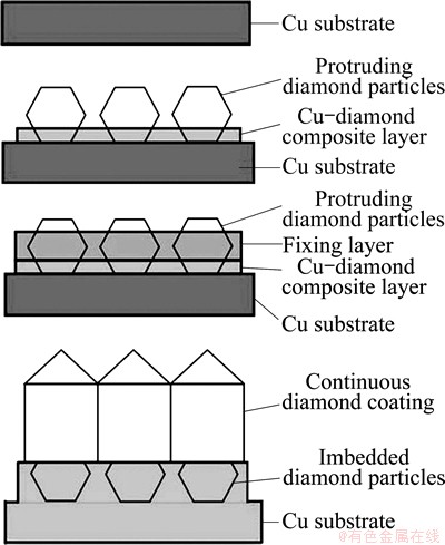
Fig. 1 Schematic diagram of fabricating adherent diamond coating on Cu substrate
All samples were characterized by a scanning electron microscope (SEM), Raman spectroscopy (Argon laser, λ=514.5 nm) and X-ray diffraction (XRD, λ=0.154 nm from Cu Kα target) to investigate the surface morphology, the crystallinity and internal stress, and the phase structure, respectively. Adhesion strength of the diamond coatings was tested by Vickers hardness tester in the load range of 9.8-147 N, using a right pyramid indenter with a square base and an angle of 136° between opposite faces.
3 Results and discussion
3.1 Surface morphology of diamond on copper
The surface morphology of the as-plated Cu-diamond composite layer on Cu substrate is shown in Fig. 2(a). Diamond particles are well distributed in the Cu matrix and no specific orientation or clear facets are observed. Most of the diamond particles are only partially embedded in the matrix. Figure 1(b) shows that the embedded depth exceeds half size of diamond particles and the embedded portions are firmly anchored in the copper matrix. This feature is highly desirable, since the uncovered portion can serve as the seed for subsequent CVD homo-epitaxial or second nuclei diamond growth, which can improve the adhesion between substrate and diamond film. It must be noticed that the overplating has to be avoided, since the diamond grains covered with copper will no longer act as the nucleation centers for CVD diamond growth. It is estimated by SEM that the area coverage of the diamond particles is 35%-40%, and the particle density is about 2×105 cm-2. The later is much lower than that of pretreatment of abrading substrate with diamond powder, which is about 1011 cm-2 [14] in the size of 5-30 nm. The obtained interlayer structure is beneficial for improving the interfacial strength, but disadvantageous for forming continuous diamond film during CVD growth.
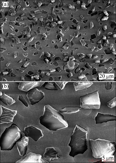
Fig. 2 SEM images showing distribution of diamond particles (a) and diamond particle embedded in Cu layer (b)
As expected, the experiments showed that the diamond coating can firmly adhere to substrate after slowly cooling process. The surface morphology of the diamond film on Cu-diamond composite coated copper substrate after 20 h deposition by hot-filament CVD is shown in Fig. 3(a). The continuous diamond coating grains are composed of both large and small well-faceted diamond grains. The large grains with size of 20-25 μm are in cubo-octahedron or modified cubo-octahedron shape with triangular and square planes. More often, the square planes contain small second nuclei (white arrow in Fig. 3(b)). The small grains with size of 1-5 μm and triangular apparent facets (Fig. 3(b)) fill in the gaps between the large grains and form continuous diamond film.
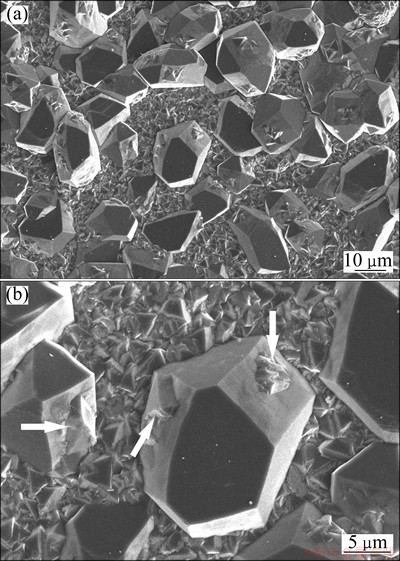
Fig. 3 SEM images showing surface morphology of diamond coating (a) and second nuclei grains filled in gaps of large diamond grains (b)
The cubo-octahedron shape of large diamond particles observed in this experiment suggests that it is a middle growth shape for the irregular diamond seeds converting to octahedron grains in the CVD growing process. As well established for the crystallography of diamond growth, the triangular crystallographic plane is (111) and the square is (100) [15,16]. The minimum and secondary low specific surface energy planes for diamond are (111) and (100), respectively. Based on the thermodynamics theory, the preferred diamond grain shape with the lowest Gibbs free energy is octahedron composed of (111) crystallographic planes, not cubo- octahedron composed of (111) and (100) faces. Based on the kinetic theory, the growth shape of diamond particle at different stages of CVD growth is dependent on the relative growth rates of constituent crystallographic planes [16]. Under certain conditions, a high-index crystal plane having higher specific surface energies generally has a higher growth rate. The quickly growing planes gradually decrease their areas, while slowly growing planes increase their areas [17]. The size of diamond seeds in Fig. 2 is two-order magnitude larger than that of diamond films pretreated by abrading substrate with diamond powder. The large surface of the irregular diamond seeds could be considered the cover of a large number of any index crystal planes. The higher the index planes with high specific surface energy are, the faster the planes disappear. The shape of diamond seeds gradually changed from irregular to cubo- octahedron shape and finally to the equilibrium octahedron shape with the increase of the CVD growth time. When the grain changed into cubo-octahedron or modified cubo- octahedron shape, the grain size was 20-25 μm. Further growth for converting to octahedron requires the growth species (such as CH3― and CH2―, decomposed from the hot filament) to diffuse along distance to the kink or ledge on (100) planes. This requires high substrate temperature and low CH4 concentration to guarantee the diffusive activity of growth species. On the contrary, relative low substrate temperature and high CH4 concentration will result in the second nuclei growth on (100) planes, as shown in Fig. 3(b).
The small particles filled in the gaps between the large diamond grains were proposed to come from the lateral second nucleation on dihedral angle between the large diamond grain and copper substrate. The well established diamond growth mechanism points out that the hydrocarbon species preferentially homo-epitaxially grows on diamond seeds rather than hetero-nucleation for the high surface energy of diamond [14]. The mechanism of the lateral second nucleation is schematically shown in Fig. 4. The growth species such as CH3― and CH2― from the hot filament are absorbed by both diamond seeds and copper substrate. The species on seeds surface diffused to high-index planes for homo-epitaxial growth and the species on copper needed to diffuse to diamond seed surface. The diamond seed density in Fig. 2 is 5-order magnitude less than that of the films pretreated by abrading substrate with diamond powder, though the size of the former is 2 orders magnitude larger. This means that the width between two seeds on the Cu-diamond layer is much larger than that of the pretreatment of abrading substrate with diamond powder and the species need much longer diffusion distance to meet the seeds. Some of the species condensed at high energy points (such as scratches, pits) and formed hetero-nucleus of diamond, and the others diffused to dihedral angle between diamond grain and copper substrate. If the substrate temperature is high enough, the species from copper could continuously diffuse to high energy planes for the homo-epitaxial growth. If the temperature is not high enough, the species would condense at dihedral angle where both diamond and copper could contribute surface energy to form the second diamond nuclei. The second nuclei and hetero-nuclei can grow up quickly to micro-scale octahedral shaped grains with exposed (111) faces, which can serve as new dihedral angles for the next second nucleation and growth. The grains from second nucleation and growth eventually filled the gaps between the large diamond grains. By this way, continuous diamond film can be formed. This structure is helpful for the decrease of the holes at the copper/diamond interface.
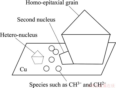
Fig. 4 Schematic diagram of lateral second nucleation on dihedral angle
3.2 Residual stress of diamond film
Figure 5 shows the Raman spectrum of the as-prepared diamond film. The strong and sharp peak at 1333.9 cm-1 represents the good crystalline nature of diamond. The shift in the peak from normal peak position of natural diamond (1332 cm-1) indicates that the film is under compressive stress. In the case of biaxial stress σ, the Raman line of polycrystalline diamond generally splits into singlet and doublets [18]. As no splitting peak is observed in Fig. 5, the peak at 1333.9 cm-1 is assumed to be an overlap of singlet and doublets, and
σ =-0.567(νm-νo) (1)
where νm and νo are wavenumber obtained from as-prepared diamond film and natural diamond, respectively. Using this equation, the compressive stress in the diamond film grown on Cu-diamond composite interlayer is calculated to be 1.08 GPa, much higher than those in Refs. [9-11]. This is mainly attributed to the insufficient stress relief for large area continuous diamond film growth. The stress can be divided into thermal stress and growth stress. Since the soft copper and slow cooling process could relieve considerable thermal stress, the total stress (1.08 GPa) was mainly from the growth stress.
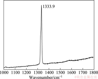
Fig. 5 Raman spectrum of diamond film grown on Cu-diamond composite layer
3.3 Adhesion between diamond film and substrate
As we know, diamond films deposited directly on copper substrate usually crack or peel off during post cooling process due to the poor bonding strength and the large mismatch of thermal expansion coefficients between diamond and copper [10,19,20]. In this work, the adhesion of the diamond film on Cu-diamond composite interlayer was evaluated by Vickers hardness tester with a right pyramid indenter of a square base and an angle of 136° between opposite faces. The load was applied by step increasing from 9.8 to 107.8 N till the delamination on the periphery of the imprint was found. The microstructures of the film after test are shown in Fig. 6. The two diagonal lengths of the imprint measured from Fig. 6(a) were 583 μm and 501 μm with the average of 542 μm. Assuming that the residual imprint has the same shape of indenter, the calculated imprint depth is about 154 μm. This imprint depth was much larger than the total thickness of diamond coating and Cu-diamond interlayer (about 35 μm), indicating that the indenter penetrated through the diamond film and Cu-diamond interlayer into copper substrate and caused the plastic deformation of the residual imprint. Only one piece of delamination area was detected on the periphery of the square imprint corner (white arrow denoted in Fig. 6(a)) after indentation test with 107.8 N load. Figure 6(b) shows the irregular pits with different sizes distributed on the delamination area, implying that the pits result from the pulling out of the diamond particles from Cu-diamond interlayer. The characteristic of pulling out deformation on the edge of pits (Fig.6 (c)) suggests that the mechanical interlock between diamond and copper increases the adhesive strength.
In order to correctly perform indentation test for adhesion measurement, the substrate should deform plastically to initiate and propagate the interface cracks between the film and substrate, interfering with the film cracking and delamination in the nearby periphery of the imprint [21]. For ductile substrate, the periphery of the indent would be sunk-in with the indenter penetrating into substrate, forming a bucking area [22] on the loading procedure of indentation test. If the adhesion strength between the coating and substrate is high enough, concentric cracks in the coating will be propagated in the bucking area. If the adhesive strength is not high enough, delamination area will be formed [12]. The total adhesive strength is composed of chemical bonding strength and mechanical interlock strength. The former is mainly attributed to the wettability between the coating and substrate. Due to the poor wettability with copper, the embedded diamond particles were pulled out from the composite interlayer, leaving the replicated morphology on the pits (see Figs. 6(b) and (c)). Though the embedded diamond particles also increase the interfacial contact area, the bonding strength does not increase significantly. Nevertheless, the continuous diamond film was successfully deposited on diamond-Cu composite layer coated on copper in this work. The improved adhesion is mainly attributed to the deep anchoring of the diamond particles in the Cu matrix.
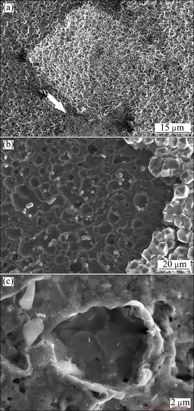
Fig. 6 SEM images of whole indentation imprint (a), distributed pits on delamination area (b), and pulling out deformation on edge of pit (c) at applied load of 107.8 N
4 Conclusions
1) Continuous diamond films with large area of 10 mm×20 mm were fabricated on copper substrate by employing a Cu-diamond composite interlayer.
2) The diamond film is composed of large cubo-octahedron grains resulting from homo-epitaxial growth and small (111) apparent facets grain from lateral second nuclei growth.
3) The improved adhesion between diamond film and substrate results from the diamond particles deeply anchored in the Cu matrix.
References
[1] YOSIDA K, MORIGAMI H. Thermal properties of diamond/copper composite material [J]. Microelectronics Reliability, 2004, 44: 303-308.
[2] SCHUBERT T, TRINDADE B,  T, KIEBACK B. Interfacial design of Cu-based composites prepared by powder metallurgy for heat sink applications [J]. Materials Science and Engineering A, 2008, 475: 39-44.
[3] YONG Tai-fa. Fabrication and thermal analysis of copper/diamond/ copper thermal spreading device [J]. Surface & Coatings Technology. 2007, 202: 1208-1213.
[4] FAN Q F, PEREIRA E, GRACIO J. Preparation of freestanding diamond films by a two-step-growth method [J]. Journal of Materials Research, 1998, 13: 2787-2790.
[5] LIU Xue-zhang, WEI Qiu-ping, ZHAI Hao, YU Zhi-ming. Enhancement of nucleation of diamond films deposited on copper substrate by nickel modification layer [J]. Transactions of Nonferrous Metals Society of China, 2013, 23: 667-673.
[6] FAN Q H, FERNANDES A, PEREIRA E, GRACIO J. Evaluation of aherence of diamond coating by indentation method [J]. Vacuum, 1999, 52: 163-167.
[7] ALI N, AHMED W, REGO C A, FAN Q H. Chromium interlayers as a tool for enhancing diamond adhesion on copper [J]. Diamond and Related Materials, 2000, 9: 1464-1470.
[8] BATTABYAL M, BEFFORT O, KLEINER S, VAUCHER S, ROHR L. Heat transport across the metal-diamond interface [J]. Diamond & Related Materials, 2008, 17: 1438-1442.
[9] HARTSELL M L, PLANO L S. Growth of diamond films on copper [J]. Journal of Materials Research, 1994, 9: 921-926.
[10] NARAYAN J, CHEN X. Laser patterning of diamond films [J]. Journal of Applied Physics, 1992, 71: 3795-3801.
[11] RAMESHAM R, ROSE F M, ALLERMAN A. Selective diamond seed deposition using electroplated copper [J]. Diamond and Related Materials, 1992, 1: 907-910.
[12] QIU W Q, DASARI A, MAI Y W. Improvement in adhesion of diamond film on Cu substrtate with an inlay structure interlayer [J]. Surface & Coatings Technology. 2011, 206: 224-227.
[13] HUANG Y S, QIU W Q, LUO C P. Effect of molybdenum on diamond deposition and adhesion [J]. Thin Solid Films, 2005, 472: 20-25.
[14] IIJIMA S, AIKAWA Y, BABA K. Growth of diamond particles in chemical vapor deposition [J]. Journal of Materials Research, 1991, 6: 1491-1497.
[15] KOBASHI K, NISHIMURA K, KAWATE Y, HORIUCHI T. Synthesis of diamonds by use of microwave plasma chemical-vapor deposition: Morphology and growth of diamond films [J]. Physical Review B, 1998, 38(6): 4067-4084.
[16] SUN B, ZHANG X, LIN Z. Growth mechanism and the order of appearance of diamond (111) and (100) facets [J]. Physical Review B, 1993, 47(15): 9816-9824.
[17] KIM J S, KIM M H, PARK S S, LEE J Y. The morphology changes in diamond synthesized by hotfilament chemical vapor deposition [J]. Journal of Applied Physics, 1990, 67: 3354-3357.
[18] AGER J W, DRORY M D. Quantitative measurement of residual biaxial stress by Raman spectroscopy in diamond grown on Ti alloy by chemical vapor deposition [J]. Physical Review B, 1993, 48(4): 2601-2067.
[19] FAN Q H, GRACIO J, PEREIRA E. Free-standing diamond film preparation using copper substrate [J]. Diamond and Related Materials, 1997, 6: 422-425.
[20] NARAYAN J, GODBLE V P, MATERA G. Enhancement of nucleation and adhesion of diamond films on copper, stainless steel, and silicon substrates [J]. Journal of Applied Physics, 1992, 71: 966-971.
[21] JINDAL P C, QUINTO D T, WOLF G J. Adhesion measurements of chemically vapor deposited and physically deposited hard coatings on WC substrate [J]. Thin Solid Films, 1987, 154: 361-375.
[22] OLIVER W C, PHARR G M. Measurement of hardness and elastic modulus by instrumented indentation: Advances in understanding and refinements to methodology[J]. Journal of Materials Research, 2004, 19: 3-20.
邱万奇1,胡志刚1,刘仲武1,曾德长1,周克崧1,2
1. 华南理工大学 材料科学与工程学院,广州 510640;2. 广州有色金属研究院 新材料研究所,广州 510651
摘 要:在铜基体表面电沉积铜-金刚石复合过渡层,采用电镀铜加固突出基体表面的金刚石颗粒,最后利用热丝化学气相沉积(HFCVD)法在复合过渡层上沉积大面积的与基体结合牢固的连续金刚石膜。采用扫描电子显微镜、拉曼光谱和压痕试验对所沉积的金刚石膜的表面形貌、内应力及膜/基结合性能进行研究。结果表明:金刚石膜由粗大的立方八面体颗粒与细小的(111)显露面颗粒组成,细颗粒填充在粗颗粒之间,形成连续的金刚石膜。复合过渡层中的露头金刚石经CVD同质外延生长成粗金刚石颗粒,而铜表面与粗金刚石之间的二面角上的二次形核繁衍长大成细金刚石颗粒。金刚石膜/基结合力的增强主要来源于金刚石膜与基体之间形成镶嵌咬合和较低的膜内应力。
关键词:金刚石膜;复合层;电镀;粘结;化学气相沉积
(Edited by Xiang-qun LI)
Foundation item: Projects (51071070, 51271079) supported by the National Natural Science Foundation of China; Project (NCET-11-0156) supported by New Century Excellent Talents in University, China
Corresponding author: Wan-qi QIU; Tel: +86-20-87111312; E-mail: mewqqiu@scut.edu.cn
DOI: 10.1016/S1003-6326(14)63122-8

