
Influence of oxygen partial pressure on properties of N-doped ZnO films deposited by magnetron sputtering
WANG Jin-zhong(������)1, 2, E. ElANGOVAN2, N. FRANCO3,
A. ALVESE3, A. REGO4, R. MARTINS2, E. FORTUNATO2
1. School of Materials Science and Engineering, Harbin Institute of Technology, Harbin 150001, China;
2. Material Science Department, CENIMAT/I3N and CEMOP/UNINOVA, FCT-UNL,
Campus de Caparica, 2829-516 Caparica, Portugal;
3. Ion Beam Laboratory, Physics Department, Institute of Technology and
Nuclear EN. 10, 2686-953 Sacavem, Portugal;
4. Center of Molecular Chemistry-Physics, Institute of Nanoscience and Nanotechnology,
Complexo Interdisciplinar, IST 1049-001 Lisboa, Portugal
Received 13 July 2009; accepted 12 September 2010
Abstract: N-doped ZnO films were radio frequency (RF) sputtered on glass substrates and studied as a function of oxygen partial pressure (OPP) ranging from 3.0?10-4 to 9.5?10-3 Pa. X-ray diffraction patters confirmed the polycrystalline nature of the deposited films. The crystalline structure is influenced by the variation of OPP. Atomic force microscopy analysis confirmed the agglomeration of the neighboring spherical grains with a sharp increase of root mean square (RMS) roughness when the OPP is increased above 1.4?10-3 Pa. X-ray photoelectron spectroscopy analysis revealed that the incorporation of N content into the film is decreased with the increase of OPP, noticeably N 1s XPS peaks are hardly identified at 9.5?10-3 Pa. The average visible transmittance (380-700 nm) is increased with the increase of OPP (from ~17% to 70%), and the optical absorption edge shifts towards the shorter wavelength. The films deposited with low OPP (�� 3.0?10-4 Pa) show n-type conductivity and those deposited with high OPP (�� 9.0?10-4 Pa) are highly resistive (> 105 W?cm)
Key words: ZnO; oxygen partial pressure; magnetron sputtering; transmittance
1 Introduction
Zinc oxide (ZnO) is a promising candidate for UV or blue light materials due to its direct wide-band-gap and large excition binding energy[1-2]. It is well established that the n-type ZnO films can be obtained rather easily in comparison with its p-type counterpart, due to the self-compensation effects and asymmetry doping in ZnO[3-4]. Many p-type doping elements such as nitrogen (N), phosphorous and arsenic, have been studied, and encouraging results have been achieved[5-11]. Among these dopants, N has received much attention[12-14] since it is theoretically proven as the optimal p-type dopant for ZnO[15]. Further, the electroluminescence was observed from ZnO homo-junction by using N as the p-type dopant[5]. However, the stronger yellow-green emitting from deep energy level transition and high deposition temperature makes it be difficult to realize the application of ZnO in ultra-violet or blue light LED or LD[5-7]. It is known that the properties of the semiconductor films are affected by their growth ambient. For ZnO, its properties have been greatly influenced by oxygen[16]. However, there are few reports on the influence of oxygen on single N-doped ZnO. In order to well understand the influence of oxygen (O2) on the properties of N-doped ZnO films, the films were sputtered with different oxygen partial pressures (OPP). Although the deposited films show n-type conductivity or high resistivity, the obtained results are promising to contribute the development on the N doping in ZnO films.
2 Experimental
ZnO films were RF sputtered on glass substrates using a ceramic ZnO target (99.99% purity) with different OPP ranging from 3.0?10-4 to 9.5?10-3 Pa in Ar+N2+O2 gas mixture. For comparison, the films were also deposited without O2. The partial pressures of argon and nitrogen were maintained at ~4.4?10-1 and 4.2?10-2 Pa, respectively. The target�C substrate distance was fixed at 10 cm. The chamber was evacuated initially to be ~2?10-4 Pa prior to the initiation of deposition process. All the films were sputtered with a constant power of 100 W for 50 min. The films sputtered with the OPP of 0, 3.0?10-4, 9.0?10-4, 1.4?10-3, 2.6?10-3 and 9.5?10-3 Pa, which are denoted as S1, S2, S3, S4, S5 and S6, respectively. A radiofrequency power generator (13.6 MHz) from Advanced Energy (Model: RFX 2500) was used for sputtering the target.
The thickness of the films was measured using a surface profilometer (Dektak3) with an accuracy of �� 20 nm. The crystal structure of the films was confirmed using an X-ray diffractometer (DMAX-III C from Rigaku; sealed tube, Cu K�� radiation) in Bragg-Brentano geometry (��/2�� coupled). The chemical composition was analyzed using X-ray photoelectron spectroscopy (Al Ka radiation, 1 486.7 eV, from a Kratos SAM800). Optical transmittance was measured using a double-beam spectrophotometer (Shimadzu UV-3100). The electrical parameters were estimated using a Hall measurements setup (Bio Rad HL5500 Hall system) with a permanent magnet of 0.5 T in van der Pauw configuration. The surface morphology was analyzed using an atomic force microscope (AFM). Tapping mode AFM experiments were performed in a multimode AFM microscope coupled to a Nanoscope IIIa controller (Digital Instruments, Veeco). Commercially etched silicon tips with typical resonance frequency of ca. 300 kHz were used as AFM probes.
3 Results and discussion
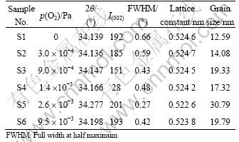
The XRD patterns were obtained from the deposited samples with the scan angle (2q) ranging from 30? to 75��. Besides the strong (100), (002) and (101) ZnO peaks, the other diffraction peaks related to ZnO are also observed, which implies that the films are polycrystalline. In order to understand well the influence of OPP on the properties of the deposited N-doped ZnO films, the XRD patterns in the 2q ranging from 30�� to 38�� are shown in Fig.1. It can be noticed that the intensity of the strongest (100), (002) and (101) peaks are significantly influenced by the variation of OPP. The (100) and (101) peaks are very weak for the samples S1 and S2; however, they become strong when the OPP is increased to �� 9.0?10-4 Pa. Their intensities are increased with the increase of OPP and reach a maximum at 2.6?10-3 Pa, but then the (100) peak disappears at the OPP of 9.5?10-3 Pa and the intensity of the (101) peaks decreases drastically. The (002) peak is the weakest for S4 deposited at OPP of 1.4?10-3 Pa. More or less than this value, the (002) peak becomes strong. The data extracted from the XRD patterns are summarized in Table 1. The extracted data suggest that the strain in ZnO films is marginally relaxed with the increase of OPP. The crystallite size is hardly varied at low OPP (�� 1.4?10-3 Pa) but then significantly increased at OPP of 2.6��10-3 Pa. The foregoing discussion suggests that the OPP plays an important role in determining the crystal structure.
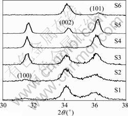
Fig.1 XRD patterns of N- doped ZnO films as function of OPP
Table 1 Summary of data extracted from XRD patterns
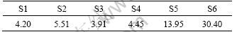
The surface microstructures obtained through AFM analysis are shown in Fig.2 (The dimensions of AFM images are 2 ��m��2 ��m). For the low OPP (�� 9.0?10-4 Pa), the surface is composed of uniformly distributed spherical grains. The ��worm-like�� grains obtained from S4 confirm the agglomeration of the neighboring grains. The agglomeration seems to be accelerated with the further increase above 1.4?10-3 Pa and the big clusters of grains are obtained. When the OPP is increased to the maximum of 9.5?10-3 Pa, the grains seem to have completely restructured to be ��leaf-like��. The obtained RMS roughness is given in Table 2. It is perceptible that the roughness is hardly changed for the films deposited at OPP �� 1.4?10-3 Pa but is significantly increased when the OPP is increased further. The evolution of the surface microstructures is in agreement with the XRD analysis, which is further authenticating the influence of OPP on the surface morphology.
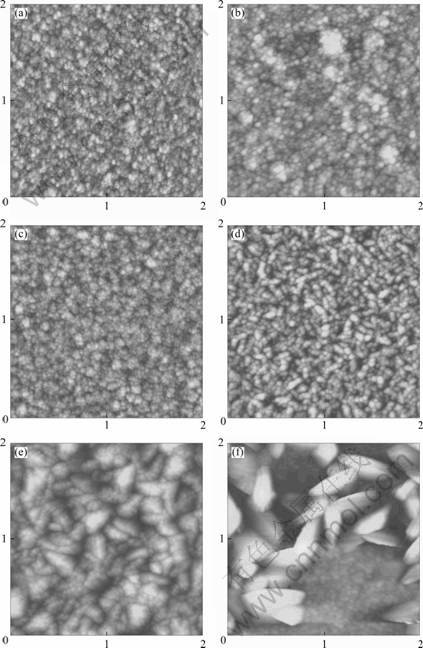
Fig.2 AFM surface microstructures obtained from N-doped ZnO films at different oxygen partial pressures: (a) 0 Pa; (b) 3.0��10-4 Pa; (c) 9.0��10-4 Pa; (d) 1.4��10-3 Pa; (e) 2.6��10-3 Pa; (f) 9.5��10-3 Pa
Table 2 RMS roughness obtained from AFM analysis (nm)
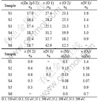
The films were analyzed using XPS technique and the mole fractions of the elements were calculated from the peak area. Fig.3 shows N 1s XPS spectra obtained from the samples S1, S3, S5 and S6. N 1s peaks are detected around 396, 398 and 399 eV, respectively. It is
noteworthy that the relative intensity of N 1s peak is decreased with the increase of OPP, and it is not detected from the samples deposited at OPP of 9.5?10-3 Pa. The composition of each element and their mole ratio obtained from the peak are quantified, as listed in Table 3. The n(N)/n(Zn) ratio indicates that the N content in the film starts to decrease significantly with the increase of OPP and eventually reaches 0 at 9.5?10-3 Pa. This variation can be related to larger electro-negation of oxygen than that of nitrogen, which makes O atoms to be incorporated (instead of N atoms) into the film during sputtering. This is further supported by the increase in mole ratio of O binding to zinc (O 1). In addition, the mole fraction of adsorbed O (O 2) is decreased above 9.0?10-4 Pa, which should be related to the decrement in surface area of the samples caused by the agglomeration of the neighboring grains. The foregoing discussion probably indicates the influence of OPP on the film composition and structure, especially at high partial pressure.
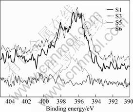
Fig.3 N 1s XPS spectra obtained from N-doped ZnO films deposited at different OPP
Table 3 Data extracted from XPS analysis
The optical transmittance spectra of the films in the wavelength ranging from 350 to 1 500 nm are recorded and shown in Fig.4. It is noteworthy that the bare substrate is placed in the reference path of the beam and hence the values refer the film transmittance alone. The average visible transmittance (wavelength ranging from 380 to 700 nm) of the films is significantly increased from 17% to 70% with the increase of OPP. This implies that the transmittance of the film is enhanced with the increase of OPP. Consequently, the optical adsorption edge is shifted towards the shorter wavelength with the increase of OPP. The optical band gap (Eg) was estimated from the plot of absorption coefficient vs photon energy, which is shown in the inset of Fig.4. The obtained values indicate that Eg is not varied until the OPP is 3.0?10-4 Pa but then starts to widen with the increase of OPP (from 2.22 eV to 3.21 eV). The obtained Eg values can be related with the variation of N content in the films caused by the increase of OPP, therein corroborating the XPS analysis.
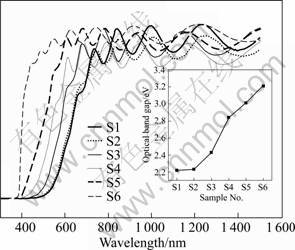
Fig.4 Comparison of transmittance spectra
The electrical properties of the samples were estimated from the room temperature Hall measurements in van der Pauw configuration. The films deposited at OPP �� 3.0?10-4 Pa (S1 and S2) show n-type conductivity. The carrier concentration of the films deposited without O2 is decreased from 2.33��1017 cm-3 to 1.87��1016 cm-3 for the OPP of 3.0��10-4 Pa, showing about one order of magnitude decrement. When the OPP is increased to �� 9.0?10-4 Pa, the films become highly resistive (r is higher than 105 W?cm) and correspondingly the Hall coefficients are not detectable. This high r is presumably due to the variation of N content and chemical states of the films that is caused by the high OPP.
4 Conclusions
1) N-doped ZnO films were RF sputtered on glass substrates and studied as a function of oxygen partial pressure (OPP). The films are polycrystalline and their crystal structures are influenced by OPP.
2) At low OPP, the film surface is composed of spherical grains. The grains start to agglomerate with the increase of OPP to be ��leaf-like�� at high partial pressure (9.5?10-3 Pa). The amount of N incorporated into the film is decreased with the increase of OPP and becomes undetectable at 9.5?10-3 Pa. The optical transmittance of the N-doped ZnO films is increased with the increase of OPP and so the optical band gap follows the same trend. The films deposited at OPP �� 3.0?10-4 Pa show n-type conductivity and those deposited with �� 9.0?10-4 Pa are highly resistive because the Hall coefficients are not detectable. Overall, the obtained properties are promising in contributing the research based on the N-doped ZnO thin films.
Acknowledgements
The authors thank the Portuguese Ministry of Science and Technology (FCT-MCTES) for offering post-doctoral fellowships through the grants SFRH/BPD/34542/2007 and SFRH/BPD/35055/2007, respectively. This work is financed by FCT-MCTES through CENIMAT-I3N.
References
[1] LOOK D C, CLAFIN B. P-type doping and devices based on ZnO [J]. Phys Status Solidi B, 2004, 241: 624-630.
[2] LOOK D C, CLAFIN B, ALIVOV Y, PARK S J. The future of ZnO light emitter [J]. Phys Status Solidi A, 2004, 201(10): 2203-2214.
[3] LEE E, KIM Y, JIN Y, CHANG K J. Compensation mechanism for N acceptors in ZnO [J]. Phy Rev B, 2001, 64: 085120.
[4] AVRUTIN V, MORKOC H, SILVERSMIT H D J. Doping asymmetry problem in ZnO: Current status and outlook [J]. Proceedings of the IEEE, 2010, 98(7): 1269-1280.
[5] TSUKAZAKI A, OHTOMO A, ONUMA T, OHTANI M, MAKINO T, SUMIYA M, OHTANI K, CHICHIBU S F, FUKE S, SEGAWA Y, OHNO H, KOINUMA H, KAWASAKI M. Repeated temperature modulation epitaxy for p-type doping and light-emitting diode based on ZnO [J]. Nature Mater, 2005, 4(1): 42-46.
[6] LIM J H, KANG C K, KIM K K, PARK I K, HWANG D K, PARK S J. UV electroluminescence emission from ZnO light-emitting diodes grown by high-temperature radiofrequency sputtering [J]. Adv Mater, 2006, 18: 2720-2724.
[7] SUN J C, ZHAO J Z, LIANG H W, BIAN J M, HU L Z, ZHANG H Q, LIANG X P, LIU W F, DU G T. Realization of ultraviolet electroluminescence from ZnO homojunction with n-ZnO/p-ZnO:As/GaAs structure [J]. Appl Phys Lett, 2007, 90: 121128.
[8] WARDLE M G, GOSS J P, BRIDDON P R. Theory of Li in ZnO: A limitation for Li-based p-type doping [J]. Phys Rev B, 2005, 71(15): 155205.
[9] ZENG Y J, YE Z Z, XU W Z, LI D Y, LU J G, ZHU L P, ZHAO B H. Dopant source choice for formation of p-type ZnO: Li acceptor [J]. Appl Phys Lett, 2006, 88(6): 062107.
[10] LIN S S, LU J G, YE Z Z, HE H P, GU X Q, CHEN L X, HUANG J Y, ZHAO B H. p-type behavior in Na-doped ZnO films and ZnO homojunction light-emitting diodes [J]. Sol State Commun, 2008, 148(1/2): 25-28.
[11] KANG H S, AHN B D, KIM J H, LIM S H, CHANG H W, LEE S Y. Structural, electrical, and optical properties of p-type ZnO thin films with Ag dopant [J]. Appl Phys Lett, 2006, 88(20): 202108.
[12] NAKAHARA K, TAKASU H, FONS P, YAMADA A, IWATA K, MATSUBARA K, HUNGER R, NIKI S. Interactions between gallium and nitrogen dopants in ZnO films grown by radical-source molecular-beam epitaxy [J]. Appl Phys Lett, 2001, 79(25): 4139-4141.
[13] WANG J Z, DU G T, ZHAO B J, YANG X T, ZHANG Y T, MA Y, LIU D L, CHANG Y C, WANG H S, YANG H J, YANG S R. Epitaxial growth of NH3-doped ZnO thin films on <02-24> oriented sapphire substrates [J]. J Cryst Growth, 2003, 255: 293-297.
[14] WANG J Z, SALLET V, JOMARD F, REGO A, ELANGOVAN E, MARTINS R, FORTUNATO E. Influence of the reactive N2 gas flow on the properties of RF-sputtered ZnO thin films [J]. Thin Solid Films, 2007, 515: 8780-8784.
[15] KOBAYASHI A, SANKEY O F, DOW J D. Deep energy levels of defects in the wurtzite semiconductors AIN, CdS, CdSe, ZnS, and ZnO [J]. Phys Rev B, 1983, 28(2): 946-956.
[16] LIN B X, FU Z X, JIA Y B. Green luminescent center in undoped zinc oxide films deposited on silicon substrates [J]. Appl Phys Lett, 2001, 79(7): 943-945.
(Edited by LI Xiang-qun)
Corresponding author: WANG Jin-zhong; Tel: +86-451-86418745; E-mail: jinzhong_wang@hit.edu.cn
DOI: 10.1016/S1003-6326(10)60649-8

