Zn����CdO���ṹ�ij����ϳɼ���������
��Դ�ڿ����й���ɫ����ѧ��(Ӣ�İ�)2018���11��
�������ߣ�Milad KAVAKEBI Farid JAMALI-SHEINI
����ҳ�룺2255 - 2264
�ؼ��ʣ�Zn����CdO���ṹ������������ѧ���ܣ���ѧ����
Key words��Zn-doped CdO nanostructures; ultrasonication method; optical properties; electrical properties
ժ Ҫ����������ѧ���о�Zn���Ӷ����������ṹ�������̵�Ӱ�졣��������X��������(XRD)�ױ��������Ʊ���CdO��ƷΪ�����ṹ��������ɨ���������(FESEM)ͼ����ʾ����Ʒ��Znԭ�Ӳ���ʱ������ò�����仯�����ȱ�С���������¹��·���(PL)������-�ɼ�����(UV-Vis)���������о���Ʒ�Ĺ�ѧ���ʣ������������ͬ�ķ�����ɲ�ͬ��ԾǨ����CdO�ܴ�϶���ڲ��Ӷ��������ṹ��ѧ���ʵ��о�������Zn���ӵ��¹����������ܶ���ߣ��Ӷ�ʹ�����ṹ�ĵ�������ߣ����������ṹ�������Ĺ�����������ݱ��о��Ľ����Zn���ӿ��Ըı�CdO���ṹ���������ʡ�
Abstract: The effect of Zn dopant on the growth of cadmium oxide (CdO) nanostructures through a sonochemical method was investigated. The X-ray diffraction (XRD) patterns of the nanoparticles show CdO cubic structures for the produced samples. Field emission scanning electron microscope (FESEM) images reveal that morphologies of the samples change, when they are doped with Zn atoms, and their sizes reduce. Room temperature photoluminescence (PL) and UV-Vis spectrometers were used to study optical properties of the samples. Evaluation of optical properties indicates that different emission bands result from different transitions and the value of CdO energy band gap increases due to doping. Studies of electrical properties of the nanostructures demonstrate that Zn dopant enhances electrical conductivity and photocurrent generation as the result of light illumination on the nanostructures due to improved density of photo-generated carriers. Considering the obtained outcomes, Zn dopant can alter the physical property of the CdO nanostructures.
Trans. Nonferrous Met. Soc. China 28(2018) 2255-2264
Milad KAVAKEBI1, Farid JAMALI-SHEINI2
1. Department of Materials Science and Engineering, Ahvaz Branch, Islamic Azad University, Ahvaz, Iran;
2. Advanced Surface Engineering and Nano Materials Research Center, Department of Physics, Ahvaz Branch, Islamic Azad University, Ahvaz, Iran
Received 15 December 2017; accepted 3 June 2018
Abstract: The effect of Zn dopant on the growth of cadmium oxide (CdO) nanostructures through a sonochemical method was investigated. The X-ray diffraction (XRD) patterns of the nanoparticles show CdO cubic structures for the produced samples. Field emission scanning electron microscope (FESEM) images reveal that morphologies of the samples change, when they are doped with Zn atoms, and their sizes reduce. Room temperature photoluminescence (PL) and UV-Vis spectrometers were used to study optical properties of the samples. Evaluation of optical properties indicates that different emission bands result from different transitions and the value of CdO energy band gap increases due to doping. Studies of electrical properties of the nanostructures demonstrate that Zn dopant enhances electrical conductivity and photocurrent generation as the result of light illumination on the nanostructures due to improved density of photo-generated carriers. Considering the obtained outcomes, Zn dopant can alter the physical property of the CdO nanostructures.
Key words: Zn-doped CdO nanostructures; ultrasonication method; optical properties; electrical properties
1 Introduction
In recent years, metal oxide nanostructures, such as cadmium oxide (CdO), have been extensively considered due to their electrical and optical properties. CdO is an n-type semiconductor with a direct band gap of 2.20-2.50 eV and an indirect band gap of 1.36-1.98 eV [1-4]. Due to the special optical and electrical properties of CdO nanostructures, they have been utilized in solar cells, gas sensors, transparent electrodes and optoelectronic devices [5-9]. A variety of methods have been employed to grow CdO nanostructures. Growth techniques and types of the dopants affect physical properties of semiconductor nanostructures. So, researchers have reported different results about CdO. For example, DAKHEL [10] examined the effect of cerium (Ce) on structural, electrical and optical properties of CdO thin films deposited by vacuum evaporation technique. Their X-ray diffraction (XRD) results showed that some Ce4+ ions were substituted for Cd2+ while Ce solubility in CdO lattice was limited. Also, resistivity and optical energy band gaps of CdO were found to be decreased meantime mobility and carrier concentration were increased by Ce doping. AYDIN et al [11] synthesized aluminum (Al)-doped CdO nano-powder using sol-gel method. They observed the increase of grain size and optical energy band gap by increasing the amount of Al. In addition, in their study, electrical conductivity of un- and Al-doped samples changed due to thermal processes. BENHALILIBA et al [12] studied physical properties of un- and copper (Cu)-doped CdO thin films using sol-gel method. Small amounts of Cu improved visible light absorption of CdO from 56% to 79% and increased IR range of CdO up to 90%. Also, small amounts of Cu dopant provided very transparent films and reduced electrical resistance. VELUSAMY et al [13] investigated optical and electrical properties of praseodymium (Pr)-doped CdO thin films, which were deposited using spray pyrolysis. These films showed high transparency and mobility of electric carriers. Optical characterization identified 2.38-2.52 eV energy band gap range for the Pr-CdO films.
Using pulsed deposition and tin (Sn) dopant, ZHENG et al [14] evaluated optical and electrical properties of CdO films. Their results indicated that optical energy band gap of the Sn-doped layers is higher than that of the un-doped sample. This band gap increase continued by increasing the concentration of Sn dopant up to 2.90 eV. The results of electrical measurements showed about 3% decreased resistance of the films and about 8% increase of Sn resistance with Sn content increasing. These changes occurred due to the substitution of Cd atoms with Sn at lower Sn contents and, after that, as a result of interstitial Sn atoms. Findings have declared that physical properties of metal oxides can be changed by adding/doping different elements as dopants [15-18]. Therefore, properties of materials should be changed by selecting appropriate growth method and favorable dopant percentage. In this work, structural, electrical and optical properties of CdO prepared by a sonochemical technique are presented and discussed. Then, the CdO particles are doped with zinc (Zn) and the effects of Zn dopant on various characteristics of CdO are studied. To the best of our knowledge, there is no previous report on Zn-doped CdO particles synthesized by sonochemical technique.
2 Experimental
2.1 Raw materials
Cadmium acetate (Cd(CH3COO)2��2H2O; 99.99%), zinc acetate (Zn(CH3COO)2��2H2O; 99.99%), sodium hydroxide (NaOH) and hydrogen peroxide (H2O2) were purchased from Merck, Germany.
2.2 Experimental method
In order to grow CdO particles, 50 mmol/L (1.33 g) cadmium acetate were dissolved in 0.3 mL hydrogen peroxide and 100 mL distilled water, initially. Then, the solution was poured in a beaker and its pH was adjusted to be 8.5 using sodium hydroxide. Ultrasonic waves with 200 W power and 20 kHz frequency were applied to the solution using a titanium probe (diameter of ~12 mm) through an ultrasonic homogenizer device (Top Sonics UPH-400, 20 kHz, 400 W, Ultrasonic Technology Development Co., Iran) for 30 min with a cycle of 4 s ON and 3 s OFF. After applying ultrasonic waves, the obtained solution was filtered and the obtained sediments were washed several times with distilled water and dried at ambient temperature. To completely remove water and the other possible impurities, a heat treatment step was performed on the obtained product for 4 h, at 400 ��C and atmospheric pressure in a box furnace. In order to prepare Zn-doped CdO samples, different concentrations of zinc acetate (1, 3 and 5 mmol/L) were weighted for the samples in different beakers and added to the final solution. The remaining synthesis steps were performed similar to the procedure carried out for the un-doped sample and three doped samples, along with the un-doped samples, were prepared for analysis and characterization. To facilitate analysis of the CdO particles, the un- and Zn-doped samples with different concentrations of Zn were named Zn0, Zn1, Zn2 and Zn3, respectively.
2.3 Characterization
To check crystal quality of the grown structures, an X-ray diffractometer (X��Pert Pro, PANalytical, Netherlands) equipped with a Cu K�� anode and ��= 1.5406  was used. To study morphological properties of the CdO structures, a field emission scanning electron microscope (FESEM; Mira 3-XMU, Czech Republic) and a transmission electron microscope (TEM; EM 900, Zeiss, Germany) were used. Also, elemental analysis was performed using energy-dispersive X-ray (EDS) spectroscopy connected to the FESEM system. Moreover, for optical studies, the obtained samples were measured by a UV-Visible spectrometer (UV-Vis, Hatch 5000, UK) in the range of 300-900 nm and a photoluminescence (PL) spectrometer (PL, Perkin-Elmer LS55, USA) at room temperature and ��exc of 325 nm in the range of 200-800 nm. To study electrical properties of the CdO samples, a light-sensitive device, as a thin film, was fabricated. With this purpose, 5 mg of each sample was mixed with 0.3 mL of chitosan, as a conductive polymer. Then, a clean 1 cm �� 2 cm SiO2 substrate was considered and the prepared solution was dropped on its surface by masking it to restrict spread of the solution in 0.5 cm �� 0.5 cm area. After that, the substrate was dried in air. Two appropriate electrodes were placed on two sides of the layer using silver paste to prepare the samples for electrical experiments. Current-voltage (I-V), in darkness, and current-time (I-t) characteristics of the samples were analyzed using a special system and applying xenon light (solar cell simulator IIIS-200+, Nanosat Co., Iran; 1.5 air mass intensity (100 mW/cm2)) in intervals of 3 min ON and 3 min OFF. A bias voltage of 0.2 V was applied and its output was recorded by a Keithley source-meter 2400 (USA) system. Also, capacitance-voltage (C-V) data were recorded to plot Mott-Schottky curve by this Keithley source-meter.
3 Results and discussion
3.1 Structure
Figure 1 shows diffraction patterns of the un- and Zn-doped CdO samples. As shown in Fig. 1, the diffraction peaks thoroughly match the peaks related to cubic CdO (JCPDC card No. 03-065-2908) [19]. Details of the dominant peaks are reported in Table 1.
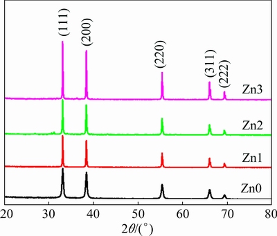
Fig. 1 XRD patterns of un- and Zn-doped CdO structures
Table 1 Specifications of dominant peak on XRD pattern for samples
Based on the data obtained from XRD analysis (Table 1), addition of Zn impurity shifts the diffraction peaks towards higher angles and reduces full width at half maximum (FWHM). The other peaks follow this trend, too. Shift in the XRD peak position is dependent on effective ionic radius of the dopant atoms [20]. If the effective ionic radius of Zn is smaller than the effective ionic radius of the host atoms (Cd), then adding Zn dopant will change peak angles of the host material towards further positions, i.e., larger angles. Since the effective ionic radius of zinc (Zn2+) is 0.74 and the effective radius of cadmium (Cd2+) is 0.95 [21], the presence of Zn is expected to change the peak positions towards higher diffraction angles, as observed in Fig. 1. The crystalline sizes of the samples are determined by the Scherrer equation [22]:
D=k��/(��hklcos ��) (1)
where D is the crystalline size in nanometers, �� is the wavelength of the radiation (1.5406 for Cu K�� radiation), k is a constant equal to 0.9, ��hkl is the peak width at half maximum intensity, and �� is the peak position. Average values of the crystallites sizes are calculated for the three main peaks and the average values of 50.50, 83.09, 97.09 and 130.68 nm are obtained for Zn0, Zn1, Zn2 and Zn3, respectively (Table 1). This implies an increase in crystallite size with enhanced Zn dopant concentration, compared with the un-doped sample. These results also show that Zn atoms have been incorporated in the crystal lattice of CdO. Shifting of the XRD peaks and changes in the intensities and distances between their crystal planes are evidences that confirm Zn incorporation.
3.2 Morphology
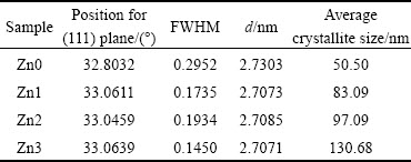
Figure 2 shows FESEM images of un- and Zn- doped CdO samples with different concentrations of Zn. As Fig. 2 illustrates, morphologies of the samples become more uniform and their particle sizes shrink with the addition of Zn dopant.
For Zn1 and Zn2 samples, cube morphologies with average diameters of (82��4) nm and (133��4) nm can be seen, respectively. However, morphology of the Zn3 sample has changed into oak tree fruit shapes. The average length and diameter of these morphologies are measured to be about (234��4) nm and (173��4) nm, respectively. Therefore, morphologies of the CdO particles become uniform by adding Zn element and increasing its concentration while they are smaller compared with the un-doped sample. Figure 3 shows the EDS spectra of the un- and Zn-doped CdO nanostructures with mass and molar fractions of elemental distributions. The EDS results reveal increased fractions of Zn in the doped samples by increasing the dopant content. Therefore, promotion of the dopant concentration in the host material structure, namely CdO, is considered to be done well, initially. Moreover, in the Zn-doped samples, as the amount of dopant increases, fraction of Cd increases and that of O decreases. In these spectra, observation of the other elements, i.e. Si and Au, is a consequence of using silicon substrate and gold coating for SEM analysis.
Transmission electron microscopy (TEM) was conducted for a comprehensive analysis of the shapes and sizes of the Zn0 and Zn1 samples. Figure 4 displays TEM images of Zn0 and Zn1 with their structure size distribution curves, which are drawn using a computer program. These images verify cubic form of CdO nanostructures. Formation of these CdO structures can be attributed to the cubic crystal lattice structure of CdO. According to Fig. 4, the structure size distribution curves show average sizes about 76.64 nm and 42.35 nm for Zn0 and Zn1, respectively. These curves, plotted using Gaussian approximation, suggest that average structure size of CdO decreases due to Zn presence, in agreement with the FESEM images. In addition, from the Scherrer equation, the crystallite size can be measured and the particles size can be estimated from the TEM. As one particle can be constituted by several crystallites, different results can be obtained from the two characterization techniques.
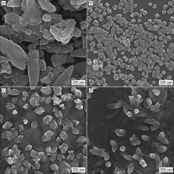
Fig. 2 FESEM images of Zn0 (a), Zn1 (b), Zn2 (c) and Zn3 (d) samples
Fig. 3 EDS spectra of Zn0 (a), Zn1 (b), Zn2 (c) and Zn3 (d) samples

Fig. 4 TEM images (a, c) and structure size histograms (b, d) of Zn0 (a, b) and Zn1 (c, d) samples
There are simple reactions that are probable for the formation of CdO nanostructures using aforementioned sonochemical method. The first reaction can be expressed by Reaction (2). It is a kind of double substitution reaction. In the second reaction, oxygen is reduced (Reaction (3)). After these two reactions, Cd cations and O anions are ready for reaction and react under appropriate conditions (ultrasonic waves) through Reaction (4).
2NaOH+Cd(CH3COO)2��2Na(CH3COO)+Cd(OH)2 (2)
H2O2��O2-+H2O (3)
Cd2++O2- CdO (Nanostructures) (4)
3.3 Optical properties
Figure 5 exhibits PL spectra of the obtained CdO samples. These spectra reflect three emission bands for the un-doped sample at 367, 481 and 733 nm, respectively. There are other emission bands, in addition to these three bands, in the un-doped samples. Emission band positioned at 367 nm (UV region) for CdO is called near band emission (NBE) since the carriers move from the valence band of CdO to its conduction band [23]. Emission bands at 481 and 733 nm (visible range) result from crystal defects in the crystal lattice of CdO [24], such as oxygen vacancies and dopants/impurities.

Fig. 5 PL spectra of un- and Zn-doped CdO nanostructures
It should be noted that no study has concerned the emission band appeared at 733 nm for CdO structures, to the best of our knowledge. In the Zn-doped samples, NBE bands have shifted to lower wavelengths (blue shift) due to changes in the amount of CdO energy band gap [25]. However, the emission band at 481 nm for the Zn-doped samples shows no shift. In the Zn-doped samples, in different emission bands, there are some other bands in addition to above three bands. All these bands are located in the visible region of electromagnetic spectrum. As stated before, these emission bands of CdO are caused by crystal defects. As expected, semiconductor doped with elements selected from the periodic table creates new bands in the electronic band structure of CdO between its conduction and valence bands. Therefore, the appearance of new emission bands upon doping CdO by Zn was predictable. Band emission intensity increases with Zn concentration whereas FWHM decreases. Energy band gap of CdO nanostructures that were grown using microwaves by SELVAM et al [26], is calculated according to their photoluminescence spectra to be around 2.52 eV. Furthermore, another band emission is observed at 430 nm, in their photoluminescence spectrum. Raspberry nanoparticles of CdO grown by NAGABHUSHANA et al [27] showed two emission bands at 527 nm and 625 nm. The first band was due to near energy gap emission and the second band was an outcome of deep trap levels caused by crystal defects.
Figure 6 shows absorption spectra of CdO nanostructures. These spectra show that the maximum absorption of all samples is in the visible region. Edges and absorption peaks in this region are well adapted to the emission spectra (PL) of the nanostructures. However, adding dopant has increased the absorption intensity. To estimate the optical band gap values of the nanostructures, the second derivative of absorption coefficient relative to energy band gap was used. In this respect, the direct band gap could be predicted from the point that the second derivative curve intersects with the energy axis from the confluence of the peak and valley with the highest intensity.

Fig. 6 UV-Vis spectra of un- and Zn-doped CdO nanostructures
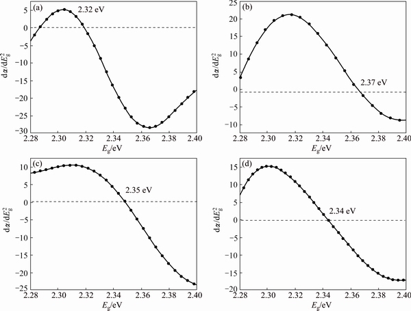
Fig. 7 Second derivative plots for estimation of optical energy band gaps of Zn0 (a), Zn1 (b), Zn2 (c) and Zn3 (d) samples
Figure 7 shows the second derivative curve for the un- and Zn-doped samples. It illustrates optical energy band gap of Zn0 to be 2.32 eV. Moreover, the band gap values of the Zn-doped samples are estimated to be 2.37, 2.35 and 2.34 eV for Zn1, Zn2 and Zn3, respectively. GUPTA et al [28] used a simple chemical precipitation method and studied energy band gap of Cu-doped CdO thin films. They observed that as Cu concentration increases, the energy band gap of CdO thin films will decrease. USHARANI and BALU [29] deposited thin films of CdO doped with different concentrations of Zn and investigated structural, optical and electrical properties of the CdO films. Tauc plot (curves of optical absorbance data ((��h��)2) versus photon energy (h��)) results showed an increase in optical energy band gap of Zn-doped CdO thin films due to the creation of additional levels at top of the energy band of CdO after doping. Therefore, in agreement with these outlined studies, the obtained values demonstrate increased optical energy band gap of CdO nanostructures after doping with Zn, compared with the pure sample. This increase can be explained by Burstein�CMoss effect that shows a blue shift in the absorption edge of doped nanostructures, as compared to un-doped nanostructures. This effect also corresponds to emission spectra of the nanostructures [29].
3.4 Electrical properties
Mott-Schottky plot is an appropriate tool for evaluating electrical properties and identifying electrical conductivity type in semiconductor nanostructures. Relying on the tangent line that is plotted on the graph and calculating its slope, information on the type of electrical conductivity and electrical carrier density can be obtained [30]. Figure 8 shows Mott-Schottky plots of the un- and Zn-doped CdO nanostructures. The positive slope of this plot indicates the nature of samples�� electrical conductivities, which means that the majority of the carries are n-type [31]. Electrical donor carrier concentration (ND) is calculated using the following equation [31]:
 (5)
(5)
where ��0 denotes permittivity constant of free space, ��s is permittivity constant of the semiconductors, e refers to charge of an electron, and S represents the slope of tangent to the point where concavity of the graph is changed. The obtained ND values of the samples are given in Table 2. The maximum value of carrier concentrations corresponds to Zn1. Therefore, it is observed that the least concentration of Zn has been able to maximize the concentration of the donor carrier. This increase of carrier concentration is in agreement with previous studies that have reported incorporation of Zn atoms in the crystal lattice of CdO. These reports have ascribed this change to Burstein-Moss effect [29,32,33].

Fig. 8 Mott-Schottky plots of Zn0 (a), Zn1 (b), Zn2 (c) and Zn3 (d) samples
Table 2 Physical parameters of CdO nanostructures

I-V characteristics of the un- and Zn-doped CdO nanostructures in symmetrical voltage range are shown in Fig. 9 to explore their electrical properties. Figure 9 depicts an ohmic behavior and suggests that higher Zn concentrations decrease electrical resistance of CdO nanostructures and increase their electrical conductivity. The observed increase in electrical conductivity maximizes for the lowest concentration of Zn and declines by increasing Zn concentration. Such behavior has been observed and reported for doping CdO with fluorine (F) [34], indium (In) [35], manganese (Mg) [36] and boron (B) [37]. These studies have attributed decreased electrical resistance and increased electrical conductivity of CdO nanoparticles doped with these elements to enhanced density and carrier mobility in CdO.
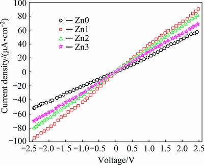
Fig. 9 I-V characteristics of un- and Zn-doped CdO nano- structures in dark condition
It is noteworthy that CdO has inherently high electrical conduction, even without doping, due to high density of the donor carriers caused by interstitial Cd atoms and O vacancies. Figure 10 demonstrates optical response of CdO nanostructures when switching ON and OFF the xenon light in 6 min periods (3 min light and 3 min darkness). Figure 10 illustrates maximum photocurrent for the sample doped with the lowest concentration of Zn and generally states that Zn dopant increases photocurrent of CdO. Mechanism of photocurrent generation in CdO has been described in detail, in our previous study [15]. Anodic current production (current shifts are positive when light is illuminated) by the un- and Zn-doped CdO samples reveals electrical conductivity nature of the dominant carriers (n-type semiconductors) [38]. This finding is consistent with the results obtained from Mott-Schottky plots. By illuminating surface of the nanostructures by light and absorbance of light photons by the nanostructures, pairs of electrons and holes produce. Some kinds of doped transition metals such as Zn can provide more negative charge carriers and/or shallow trap levels for photo-generated electron and hole so as to inhibit the recombination and enhancing charge- generation efficiency. Consequently, the photo-generated carriers causing current are allowed to pass and generate electric currents. Moreover, concerning the increase in photocurrent density by adding low concentrations of Zn and according to the results above, increasing surface to volume ratio (based on the FESEM images) and/or higher carrier concentrations (based on the Mott- Schottky) seems to play a major role [39,40].
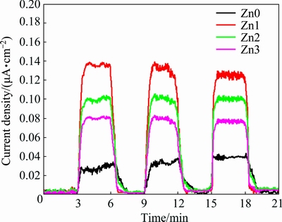
Fig. 10 Photocurrent plots of un- and Zn-doped CdO nano- structures under xenon illumination
4 Conclusions
1) The obtained XRD patterns show that Zn dopant increases crystallite size of CdO particles. Electron microscopy images indicate that CdO structures get morphologically uniformed and their sizes reduce by adding Zn dopant.
2) PL analysis identifies several emission bands that confirm the effect of Zn concentration on optical properties of CdO. Estimating optical band gap energy using the second derivative of adsorption coefficient reflects a band gap increase in the doped samples, as compared to the un-doped sample. This increase can be attributed to the Zn atoms that have been incorporated in the crystal lattice of CdO.
3) I-V curves demonstrate an ohmic behavior for the devices fabricated using the nanostructures and this feature improves electrical conductivity of the Zn-doped samples, compared to the un-doped sample. This conductivity promotion is reflected in the photocurrent results of the doped nanostructures.
Acknowledgments
Farid JAMALI-SHEINI gratefully acknowledges Ahvaz Branch, Islamic Azad University for the financial support in this research work. Authors also thank to Advanced Surface Engineering and Nano Materials Research Center, Ahvaz Branch, Islamic Azad University, Ahvaz, Iran, for the instrumentation support.
References
[1] GHOSH M, RAO C N R. Solvothermal synthesis of CdO and CuO nanocrystals [J]. Chemical Physics Letters, 2004, 393: 493-497.
[2] DONG W, ZHU C. Optical properties of surface-modified CdO nanoparticles [J]. Optical Materials, 2003, 22: 227-233.
[3] VINODKUMAR R, LETHY K J, ARUNKUMAR P R, KRISHNAN R R, PILLAI N V, PILLAI V P M, PHILIP R. Effect of cadmium oxide incorporation on the microstructural and optical properties of pulsed laser deposited nanostructured zinc oxide thin films [J]. Materials Chemistry and Physics, 2010, 121: 406-413.
[4] KUO T J, HUANG M H. Gold-catalyzed low-temperature growth of cadmium oxide nanowires by vapor transport [J]. The Journal of Physical Chemistry B, 2006, 110: 13717-13721.
[5] LI J, NI Y, LIU J, HONG J. Preparation, conversion, and comparison of the photocatalytic property of Cd(OH)2, CdO, CdS and CdSe [J]. Journal of Physics and Chemistry of Solids, 2009, 70: 1285-1289.
[6] YAKUPHANOGLU F. Nanocluster n-CdO thin film by sol�Cgel for solar cell applications [J]. Applied Surface Science, 2010, 257: 1413-1419.
[7] MANE R S, PATHAN H M, LOKHANDE C D, HAN S H. An effective use of nanocrystalline CdO thin films in dye-sensitized solar cells [J]. Solar Energy, 2006, 80: 185-190.
[8] SALUNKHE R R, LOKHANDE C D. Effect of film thickness on liquefied petroleum gas (LPG) sensing properties of SILAR deposited CdO thin films [J]. Sensors and Actuators B: Chemical, 2008, 129: 345-351.
[9] YAKUPHANOGLU F, CAGLAR M, CAGLAR Y, ILICAN S. Electrical characterization of nanocluster n-CdO/p-Si heterojunction diode [J]. Journal of Alloys and Compounds, 2010, 506: 188-193.
[10] DAKHEL A A. Effect of cerium doping on the structural and optoelectrical properties of CdO nanocrystallite thin films [J]. Materials Chemistry and Physics, 2011, 130: 398-402.
[11] AYDIN C, EL-NASSER H M, YAKUPHANOGLU F, YAHIA I S, AKSOY M. Nanopowder synthesis of aluminum doped cadmium oxide via sol-gel calcination processing [J]. Journal of Alloys and Compounds, 2011, 509: 854-858.
[12] BENHALILIBA M, BENOUIS C E, TIBURCIO-SILVER A, YAKUPHANOGLU F, AVILA-GARCIA A, TAVIRA A, TRUJILLO R R, MOUFFAK Z. Luminescence and physical properties of copper doped CdO derived nanostructures [J]. Journal of Luminescence, 2012, 132: 2653-2658.
[13] VELUSAMY P, BABU R R, RAMAMURTHI K, ELANGOVAN E, VIEGAS J, DAHLEM M S, ARIVANANDHAN M. Characterization of spray pyrolytically deposited high mobility praseodymium doped CdO thin films [J]. Ceramics International, 2016, 42: 12675-12685.
[14] ZHENG B J, LIAN J S, ZHAO L, JIANG Q. Optical and electrical properties of Sn-doped CdO thin films obtained by pulse laser deposition [J]. Vacuum, 2011, 85: 861-865.
[15] GANJIANI Z, JAMALI-SHEINI F, YOUSEFI R. Electrochemical synthesis and physical properties of Sn-doped CdO nanostructures [J]. Superlattices and Microstructures, 2016, 100: 988-996.
[16] SHEINI F J, SINGH J, SRIVASATVA O N, JOAG D S, MORE M A. Electrochemical synthesis of Cu/ZnO nanocomposite films and their efficient field emission behaviour [J]. Applied Surface Science, 2010, 256: 2110-2114.
[17] JAMALI-SHEINI F, MORE M A, JADKAR S R, PATIL K R, PILLAI V K, JOAG D S. Observation of photoconductivity in Sn-doped ZnO nanowires and their photoenhanced field emission behavior [J]. The Journal of Physical Chemistry C, 2010, 114: 3843-3849.
[18] MONTAZERI A, JAMALI-SHEINI F. Enhanced ethanol gas-sensing performance of Pb-doped In2O3 nanostructures prepared by sonochemical method [J]. Sensors and Actuators B: Chemical, 2017, 242: 778-791.
[19] ICDD X-ray diffraction clinics [EB/OL]. http://www.icdd.com. 1997.
[20] YOUSEFI R, CHERAGHIZADE M, JAMALI-SHEINI F, MAHMOUDIAN M R, SAAEDI A, HUANG N M. Influences of anionic and cationic dopants on the morphology and optical properties of PbS nanostructures [J]. Chinese Physics B, 2014, 23: 108101.
[21] SHANNON R D. Revised effective ionic radii and systematic studies of interatomic distances in halides and chalcogenides [J]. Acta Crystallogr Sect A: Cryst Phys Diffr Theor Gen Crystallogr, 1976, 32: 751-767.
[22] DANISH R, AHMED F, ARSHI N, ANWAR M S, KOO B H. Facile synthesis of single-crystalline rutile TiO2 nano-rods by solution method [J]. Transactions of Nonferrous Metals Society of China, 2014, 24: s152-s156.
[23] THEMA F T, BEUKES P, GURIB-FAKIM A, MAAZA M. Green synthesis of Monteponite CdO nanoparticles by Agathosma betulina natural extract [J]. Journal of Alloys and Compounds, 2015, 646: 1043-1048.
[24] KAVIYARASU K, MANIKANDAN E, KENNEDY J, JAYACHANDRAN M. Quantum confinement and photoluminescence of well-aligned CdO nanofibers by a solvothermal route [J]. Materials Letters, 2014, 120: 243-245.
[25] ASWANI T, PUSHPA MANJARI V, BABU B, MUNTAZ BEGUM S, RAMA SUNDARI G, RAVINDRANADH K, RAVIKUMAR R V S S N. Spectral characterizations of undoped and Cu2+ doped CdO nanopowder [J]. Journal of Molecular Structure, 2014, 1063: 178-183.
[26] SELVAM N C S, KUMAR R T, YOGEENTH K, KENNEDY L J, SEKARAN G, VIJAYA J J. Simple and rapid synthesis of cadmium oxide (CdO) nanospheres by a microwave-assisted combustion method [J]. Powder Technology, 2011, 211: 250-255.
[27] NAGABHUSHANA H, BASAVARAJ R B, PRASAD B D, SHARMA S C, PREMKUMAR H B, VIJAYAKUMAR G R. Facile EGCG assisted green synthesis of raspberry shaped CdO nanoparticles [J]. Journal of Alloys and Compounds, 2016, 669: 232-239.
[28] GUPTA R K, YAKUPHANOGLU F, AMANULLAH F M. Band gap engineering of nanostructure Cu doped CdO films [J]. Physica E: Low-dimensional Systems and Nanostructures, 2011, 43: 1666-1668.
[29] USHARANI K, BALU A R. Structural, optical, and electrical properties of Zn-doped CdO thin films fabricated by a simplified spray pyrolysis technique [J]. Acta Metallurgica Sinica (English Letters), 2015, 28: 64-71.
[30] JAMALI-SHEINI F, CHERAGHIZADE M, NIKNIA F, YOUSEFI R. Enhanced photovoltaic performance of tin sulfide nanoparticles by indium doping [J]. MRS Communications, 2016, 6: 421-428.
[31] JAMALI-SHEINI F, CHERAGHIZADE M, YOUSEFI R. SnS nanosheet films deposited via thermal evaporation: The effects of buffer layers on photovoltaic performance [J]. Solar Energy Materials and Solar Cells, 2016, 154: 49-56.
[32] DAKHEL A A. Structural and optoelectronic properties of Zn-incorporated CdO films prepared by sol-gel method [J]. Journal of Alloys and Compounds, 2012, 539: 26-31.
[33] ZIABARI A A, GHODSI F E. Optoelectronic studies of sol-gel derived nanostructured CdO-ZnO composite films [J]. Journal of Alloys and Compounds, 2011, 509: 8748-8755.
[34] SANTOS-CRUZ J, TORRES-DELGADO G, CASTANEDO- PEREZ R, ZUNIGA-ROMERO C I, ZELAYA-ANGEL O. Optical and electrical characterization of fluorine doped cadmium oxide thin films prepared by the sol-gel method [J]. Thin Solid Films, 2007, 515: 5381-5385.
[35] FLORES M A, CASTANEDO R, TORRES G, ZELAYA O. Optical, electrical and structural properties of indium-doped cadmium oxide films obtained by the sol-gel technique [J]. Solar Energy Materials and Solar Cells, 2009, 93: 28-32.
[36] BILGIN V, AKYUZ I, KOSE S, ATAY F. Characterization of Mn-incorporated CdO films grown by ultrasonic spray pyrolysis [J]. Semiconductor Science and Technology, 2006, 21: 579-585.
[37] YAKUPHANOGLU F. Synthesis and electro-optic properties of nanosized-boron doped cadmium oxide thin films for solar cell applications [J]. Solar Energy, 2011, 85: 2704-2709.
[38] SAKAI N, EBINA Y, TAKADA K, SASAKI T. Photocurrent generation from semiconducting manganese oxide nanosheets in response to visible light [J]. The Journal of Physical Chemistry B, 2005, 109: 9651-9655.
[39] JIN Y, WANG J, SUN B, BLAKESLEY J C, GREENHAM N C. Solution-processed ultraviolet photodetectors based on colloidal ZnO nanoparticles [J]. Nano Letters, 2008, 8: 1649-1653.
[40] NIKNIA F, JAMALI-SHEINI F, YOUSEFI R. Examining the effect of Zn dopant on physical properties of nanostructured SnS thin film by using electrodeposition [J]. Journal of Applied Electrochemistry, 2016, 46: 323-330.
Milad KAVAKEBI1, Farid JAMALI-SHEINI2
1. Department of Materials Science and Engineering, Ahvaz Branch, Islamic Azad University, Ahvaz, Iran;
2. Advanced Surface Engineering and Nano Materials Research Center, Department of Physics, Ahvaz Branch, Islamic Azad University, Ahvaz, Iran
ժ Ҫ����������ѧ���о�Zn���Ӷ����������ṹ�������̵�Ӱ�졣��������X��������(XRD)�ױ��������Ʊ���CdO��ƷΪ�����ṹ��������ɨ���������(FESEM)ͼ����ʾ����Ʒ��Znԭ�Ӳ���ʱ������ò�����仯�����ȱ�С���������¹��·���(PL)������-�ɼ�����(UV-Vis)���������о���Ʒ�Ĺ�ѧ���ʣ������������ͬ�ķ�����ɲ�ͬ��ԾǨ����CdO�ܴ�϶���ڲ��Ӷ��������ṹ��ѧ���ʵ��о�������Zn���ӵ��¹����������ܶ���ߣ��Ӷ�ʹ�����ṹ�ĵ�������ߣ����������ṹ�������Ĺ�����������ݱ��о��Ľ����Zn���ӿ��Ըı�CdO���ṹ���������ʡ�
�ؼ��ʣ�Zn����CdO���ṹ������������ѧ���ܣ���ѧ����
(Edited by Bing YANG)
Corresponding author: Farid JAMALI-SHEINI; Tel: +98-916-1114457; E-mail: faridjamali@iauahvaz.ac.ir, faridjamali2003@yahoo.com
DOI: 10.1016/S1003-6326(18)64870-8

