Strain induced changes in performance of strained-Si/strained-Si1-yGey/relaxed-Si1-xGex MOSFETs and circuits for digital applications
��Դ�ڿ������ϴ�ѧѧ��(Ӣ�İ�)2017���6��
�������ߣ�Kumar Subindu Kumari Amrita Das Mukul K
����ҳ�룺1233 - 1244
Key words��complementary metal-oxide-semiconductor (CMOS); high-k dielectric material; inverter; metal-oxide-semiconductor field-effect transistors (MOSFETs); SiGe; series resistance; strain
Abstract: Growing a silicon (Si) layer on top of stacked Si-germanium (Ge) compressive layer can introduce a tensile strain on the former, resulting in superior device characteristics. Such a structure can be used for high performance complementary metal-oxide-semiconductor (CMOS) circuits. Down scaling metal-oxide-semiconductor field-effect transistors (MOSFETs) into the deep submicron/nanometer regime forces the source (S) and drain (D) series resistance to become comparable with the channel resistance and thus it cannot be neglected. Owing to the persisting technological importance of strained Si devices, in this work, we propose a multi-iterative technique for evaluating the performance of strained-Si/strained-Si1-yGey/relaxed-Si1-xGex MOSFETs and its related circuits in the presence of S/D series resistance, leading to the development of a simulator that can faithfully plot the performance of the device and related digital circuits. The impact of strain on device/circuit performance is also investigated with emphasis on metal gate and high-k dielectric materials.
Cite this article as: Kumar Subindu, Kumari Amrita, Das Mukul K. Strain induced changes in performance of strained-Si/strained-Si1-yGey/relaxed-Si1-xGex MOSFETs and circuits for digital applications [J]. Journal of Central South University, 2017, 24(6): 1233-1244. DOI: 10.1007/s11771-017-3527-4.
J. Cent. South Univ. (2017) 24: 1233-1244
DOI: 10.1007/s11771-017-3527-4

Kumar Subindu, Kumari Amrita, Das Mukul K
Department of Electronics Engineering, Indian School of Mines, Dhanbad 826004, India
 Central South University Press and Springer-Verlag Berlin Heidelberg 2017
Abstract: Growing a silicon (Si) layer on top of stacked Si-germanium (Ge) compressive layer can introduce a tensile strain on the former, resulting in superior device characteristics. Such a structure can be used for high performance complementary metal-oxide-semiconductor (CMOS) circuits. Down scaling metal-oxide-semiconductor field-effect transistors (MOSFETs) into the deep submicron/nanometer regime forces the source (S) and drain (D) series resistance to become comparable with the channel resistance and thus it cannot be neglected. Owing to the persisting technological importance of strained Si devices, in this work, we propose a multi-iterative technique for evaluating the performance of strained-Si/strained-Si1-yGey/relaxed-Si1-xGex MOSFETs and its related circuits in the presence of S/D series resistance, leading to the development of a simulator that can faithfully plot the performance of the device and related digital circuits. The impact of strain on device/circuit performance is also investigated with emphasis on metal gate and high-k dielectric materials.
Key words: complementary metal-oxide-semiconductor (CMOS); high-k dielectric material; inverter; metal-oxide-semiconductor field-effect transistors (MOSFETs); SiGe; series resistance; strain
1 Introduction
For several decades, geometric scaling of devices has been considered an ultimate path for improving the performance of conventional silicon (Si) metal-oxide- semiconductor field-effect transistors (MOSFETs) [1, 2]. With excessive scaling, physical limits are governed by device physics and material properties, making it difficult to sustain the performance enhancement of devices in deep sub-micron regime [1-3]. To address these challenges, new materials and device architectures having enhanced carrier transport properties have been introduced [3-5]. Introducing strain in MOSFET has been considered a prime technology booster resulting in high performance complementary metal-oxide- semiconductor (CMOS) devices due to enhanced mobility of both electrons and holes compared to unstrained devices. Two basic techniques which are generally used for incorporating strain in conventional Si, are classified as substrate induced and local process induced techniques [6]. Strain can be introduced directly into the substrate by growing an epitaxial layer of Si on relaxed silicon-germanium (SiGe) substrate, also referred to as global strain [4, 6]. Another method includes uniaxial strain, through local process induced techniques using stressed contacts and metal gates [6, 7], stress memorization techniques [6-8], embedded source(S)/ drain(D) stressors [7, 9, 10], and so on. Strain modifies the band structure of Si, resulting in suppressed inter- valley scattering and reduced in-plane effective mass, leading to mobility enhancement which can be calculated by the ratio of mobilities of charge carriers in strained and conventional Si MOSFETs. An approximate mobility enhancement of 80% for electrons and 60% for holes has been obtained in strained-Si (s-Si) grown upon relaxed SiGe virtual substrate (VS) [11, 12]. Although a high performance gain has been achieved with such structure, the mobility enhancement for p-MOS is less compared to n-MOS and a high value of strain is required to obtain hole mobility comparable to electrons [13, 14]. It has also been reported [14, 15] that the hole mobility enhancement reduces under high transverse effective field. In order to overcome this problem, and to boost hole mobility, a compressively strained-Si1-yGey (s-Si1-yGey) layer can be grown over a relaxed-Si1-xGex (r-Si1-xGex) layer (y>x) and capped with a tensile s-Si layer. Such structure (s-Si/s-Si1-yGey/ r-Si1-xGex) is referred as dual channel (DC) heterostructure [12-17]. The subscripts x and y denote the Ge mole fraction of relaxed and strained SiGe layer respectively. Band offsets between the tensile s-Si layer and compressively strained-Si1-yGey layer can be used for the generation of high electron mobility in n-channel surface and high hole mobility in the buried p-channel MOSFETs [18]. In s-Si/s-Si1-yGey/r-Si1-xGex MOSFETs, hole mobility enhancement results from the splitting of valence band degeneracy and reduction in in-plane and out-of-plane effective mass due to compressive strain in s-Si1-yGey layer [15, 19]. Such structure with enhanced n- and p-channel performance can be used for obtaining high performance CMOS circuits. The enhancement in carrier mobility boosts the drive current of both s-Si n- and p-MOS and is higher than their unstrained counterparts. The drive current further enhances as the channel length progresses into the nanometer regime. Channel length scaling results in reduction of several device dimensions but the S/D series resistance (RSD) has not been proportionately scaled, and has become an appreciable fraction of the total resistance [1, 20, 21]. The detrimental effects of S/D series resistance increase with scaling into the deep sub-micron/nanometer regime. Presence of RSD decreases the terminal voltages of intrinsic devices limiting the device performance [20]. It has also been reported [1] that the incorporation of RSD reduces the drive current of s-Si MOSFETs by approximately 30%. Efforts have been made by various research groups to analytically model the threshold voltage [16, 22, 23], mobility and drain current [22] of intrinsic s-Si/s-Si1-yGey/r-Si1-xGex n- and p-MOSFETs, without incorporating S/D series resistance.
An inverter is the backbone of CMOS digital circuits. The voltage transfer characteristic (VTC) curve of a CMOS inverter is an important DC characteristic which expresses the electrical function of the gate in a better way [24]. Information about several other important parameters such as inverter logic threshold voltage (Vinv), noise margin (NM) and dynamic current (Icc) can be obtained from the VTC curve. The propagation delay (PD) is another performance metric which has received considerable attention through years. Both VTC and PD are heavily influenced by the drive current, the solution of which is not straight forward in the presence of series resistance. The analysis of such performance parameter is traditionally carried out with the help of circuit simulators [25, 26] and technology computer aided design (TCAD) tools [27, 28]. The framework of such tools may not be of much concern at the user end. Developing a computational technique for analyzing the performance parameters of s-Si/s-Si1-yGey/ r-Si1-xGex MOSFET-based CMOS inverters would be interesting as it may be helpful for gaining an insight of the device as well as its associated circuit. Quite surprisingly, we were not able to find much evidence of earlier theoretical work emphasizing the impact of strain and high-k dielectric material on the performance of CMOS digital circuits. Based on the above and owing to the persisting technological importance of strained Si devices [23, 29-31], the purpose of this work is two-fold: 1) Firstly, we have proposed a simulator based on multiple iterations of transcendental equations for s-Si/s-Si1-yGey/r-Si1-xGex MOSFETs as it is necessary to incorporate the S/D series resistance, and 2) we then utilize the proposed methodology to investigate the impact of strain and other device parameters on the device/CMOS circuit performance, with emphasis on metal gates and high-k dielectric materials.
2 Theoretical details
Figure 1 shows the schematic representation of s-Si/s-Si1-yGey/r-Si1-xGex MOSFET along with the S and D series resistances and nodal voltages. In dual channel heterostructure CMOS, the n-MOS channel is formed at the tensile s-Si layer for positive gate bias. For negative gate bias, the p-MOS channel is first formed in the compressively strained-Si1-yGey layer and later at the tensile s-Si layer [22]. The presence of compressively strained-Si1-yGey buried p-channel layer does not reduce the electron mobility in surface s-Si layer [12]. The intrinsic parameters of the device have been represented with subscript ��int�� as shown in association with the terminal voltages in Fig. 1. The intrinsic voltages for n-channel MOSFETs, in the presence of RSD, can be represented as
 (1)
(1)
 (2)
(2)
 (3)
(3)
where RSD,n=RS,n+RD,n, with RS,n=RD,n and ID,n is the drain current of n-channel MOSFET. Earlier works on the modeling of threshold voltage and drain current were focused on intrinsic strained devices which need to be remodeled in order to incorporate S/D series resistance as it is necessary to frame our algorithms.

Fig. 1 Schematic representation of s-Si/s-Si1-yGey/r-Si1-xGex MOSFET showing S/D series resistance along with nodal voltages
2.1 Threshold voltage
In MOSFET, strong inversion occurs when the condition for threshold is satisfied. The gate voltage, at which the electron concentration at the s-Si/SiO2 interface and the hole concentration at the s-Si/s-Si1-yGey heterointerface become equal to the substrate doping concentration (NA and ND respectively), is termed as the threshold voltage for n- and p-channel s-Si/s-Si1-yGey/ r-Si1-xGex MOSFETs, respectively [22]. The remodeling of threshold voltage is in line-up with the earlier works of BINDU et al [22] for intrinsic devices. Integrating 1-D Poisson equation and obtaining the electric field at s-Si/SiO2 interface (for n-MOS) and s-Si/s-Si1-yGey heterointerface (for p-MOS) [22], the expression of threshold voltage in the presence of S/D series resistance can be written as

 (4)
(4)
where

 (5)
(5)

 (6)
(6)

 (7)
(7)
and
 (8)
(8)
In the above equations VFB,n(p) and fth,n(p) are, respectively, the flat band voltage and the value of surface potential [22] at which strong inversion occurs (at s-Si/SiO2 interface for n-MOS and s-Si/s-Si1-yGey heterointerface for p-MOS), for n (p)-channel s-Si/s-Si1-yGey/r-Si1-xGex MOSFET. The parameters ��Si, R��1, R��2,tSiGe,n(p), tbuff,n(p), tcap,n(p) and Wm,n(p) are the permittivity of Si, ratio of permittivities of Si and s-Si1-yGey, ratio of permittivities of Si and r-Si1-xGex, thickness of s-Si1-yGey layer, thickness of r-Si1-xGex buffer layer, thickness of s-Si cap layer and maximum depletion width of n (p)-MOS respectively. f(ID,n(p)RSD,n(p)) represents the IDRSD dependence of any parameter for n (p)-MOS. We have followed this convention throughout the manuscript. Cn is the gate oxide capacitance of n-MOS and  where Ccap,p and Cox,p are the capacitance per unit area of s-Si cap layer and gate oxide of p-MOS respectively.
2.2 Drain current
The drain current of an intrinsic MOSFET can be expressed as the sum of drift and diffusion component. The drift component is the dominant one in the strong inversion region of the MOSFET operation. Following Ref. [22], the drain current expression in the linear and saturation region can be obtained by solving the drift component using suitable boundary conditions. By utilizing Eq. (1) and Eq. (2), the drain current in the linear region of the MOSFET in the presence of RSD,n(p) can then be expressed as

 (9)
(9)
where

 (10)
(10)
is the transconductance parameter.

 (11)
(11)

 (12)
(12)
In the above equations Ln(p), Wn(p) and vsat,n(p) denote, respectively, the channel length, width and saturation velocity for n (p)-channel MOSFET. ��n(p)[f(ID,n(p)RSD,n(p))] is the mobility of n (p)-channel s-Si/s-Si1-yGey/r-Si1-xGex MOSFET and is expressed as

 (13)
(13)
where ��max,n(p) is the maximum low field mobility in s-Si for n-MOS (strained-Si1-yGey layer for p-MOS). The parameter ��n(p)[f(RSD,n(p))]=��0,n(p)+(��max,n(p)Wn(p)Cn(p)RSD,n(p))/ Ln(p), is the scattering constant [32] which gets modified after inclusion of S/D series resistance. ��0,n(p) is the scattering constant for the intrinsic device. The +ve and �Cve signs appearing in the above equations correspond to n- and p-channel MOSFET respectively.
At saturation, when the pinch-off condition is reached, the electron (hole) velocity is saturated at vsat,n(p) at the drain end of the channel. Following Ref. [22] and utilizing Eq. (1) and Eq. (2), the modified extrinsic saturated drain current for n (p)-channel s-Si/s-Si1-yGey/ r-Si1-xGex MOSFET can be remodeled as


 (14)
(14)
where


 (15)
(15)

 (16)
(16)
When drain voltage increases, the pinch-off point moves towards the source. This reduces the effective channel length and the effect is known as channel length modulation, which further modifies the saturated drain current of the extrinsic device, which can be expressed as

 (17)
(17)
Figure 2(a) shows the schematic representation of a generalized CMOS inverter. The S/D series resistance associated with the device is depicted in the same figure. A generalized VTC curve of the CMOS inverter, showing various regions of operation along with the input and output voltages, is depicted in Fig. 2(b). The inverter circuit uses s-Si/s-Si1-yGey/r-Si1-xGex MOSFETs. In Fig. 2(b), VIL(IH) is the maximum (minimum) input voltage which can be interpreted as logic ��0 (1)��. Similarly VOL and VOH are the minimum and maximum output voltages which can be interpreted as logic ��0�� and ��1��, respectively. The NML and NMH can then be defined as VIL�CVOL and VOH�CVIH, respectively. These along with the inverter logic threshold voltage characterize the DC input-output characteristics of the inverter circuit.
3 Computational methodology
3.1 Mobility and drain current
Through Eqs. (4)-(17), it can be seen that introducing S/D series resistance compels several parameters to be expressed as a function of drain current. The solution of such equations is not straight forward due to the transcendental nature of drain current and hence an iterative technique has been used for the determination of various performance parameters of the inverter under consideration. Figure 3 represents the flow for calculating the drain current, threshold voltage and mobility of s-Si/s-Si1-yGey/r-Si1-xGex MOSFET incorporating S/D series resistance. To judge the accuracy of our algorithm, we have validated our computed mobilities of s-Si/s-Si1-yGey/r-Si1-xGex n- and p-MOS with the experimental work of JUNG et al [17] and RIM et al [33]. We now describe the process of validation for p-MOS. The values of ��max,p and ��p used for validation were extracted by plotting the reported data (mobility vs effective field, Eeff) [33] in Origin (OriginLab Professional V9.0. Northampton, MA) and using a curve fitting technique (ReciprocalMod Non- linear curve fit), the following expression was obtained
 (18)
(18)
Comparing Eq.(13) and Eq. (18), values of ��max,p and ��p can be obtained as ��max,p=a and ��p=b. The S/D series resistance of p-MOS was extracted from Ref. [33] following the procedure described in Ref. [21]. Using these values along with the parameters reported in Ref. [33], the plot of mobility of holes for different effective electric field was obtained using our algorithm, as depicted in Fig. 4(a) along with the reported one. In a similar way the plot of mobility for n-MOS was also obtained, as depicted in Fig. 4(b), and compared with the reported one in Ref. [17]. The average deviations lie within 5%. To further validate our work, we have also calculated the drain current of s-Si/s-Si1-yGey/r-Si1-xGex n- and p-MOSFET with the parameters mentioned in Ref. [22] and also depicted in Table 1. The same one has been plotted with drain to source voltage for different gate overdrive voltages, as shown in Figs. 5(a) and (b). Two sets of parameters are listed in Table 1 corresponding to inverter-I and II. Figures 5(a) and (b) are computed utilizing the parameters of inverter-II and I respectively. The results of our computation are compared with the reported results in the same figure. The value of the series resistance used in our computation has been extracted from the ratio of two linear I-V characteristics at low VDS for n- [34] and p-MOS [35] following the approach mentioned in Ref. [21]. Our results are in good agreement with the reported ones and the average deviation is within 5%. Through our computations, it has also been found that, incorporating RSD decreases the drain current of n-MOS by 36.4%, which is in consistent with that in Ref. [1]. The computational time of our proposed algorithm has been compared with SPICE simulation including the model parameters of BSIM 4.8.0 [36] for strained MOSFETs and introducing two external resistances in the S/D nodes. The time taken for the computation of drain current of n- and p-MOS was 0.55 s and 0.56 s, respectively. As compared to this, the computational time of our algorithm, using MATLAB (MATLAB R2013a. Natick, MA, USA: The MathWorks Inc), was 0.46 s and 0.48 s, respectively, for n- and p-MOS.
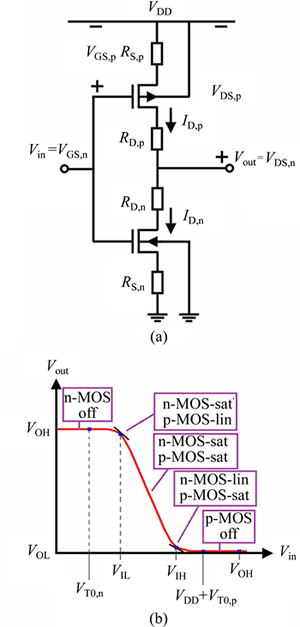
Fig. 2 Schematic representation of a CMOS inverter showing S/D series resistance (a) and a generalized VTC curve of a CMOS inverter showing various regions of operation (b)

Fig. 3 Flowchart depicting a step-wise algorithm for computing drain current of s-Si/s-Si1-yGey/r-Si1-xGex n- and p-MOSFET
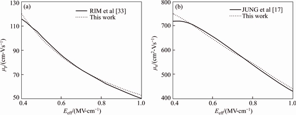
Fig. 4 Validation of computed mobility (dashed line) of s-Si/s-Si1-yGey/r-Si1-xGex MOSFET with reported data (solid line) [17, 33] for p-MOS (a) and n-MOS (b)
Table 1 Device parameters used for calculation [22]


Fig. 5 Validation of drain current (dotted line) of s-Si/s-Si1-yGey/r-Si1-xGex MOSFET with two reported data (solid [34, 35] and dashed lines [22]) for n-MOS (a) and p-MOS (b)
3.2 Voltage transfer characteristics
The drain current calculated through the algorithm of Fig. 3 can be used to obtain the VTC curve. As the plot of VTC depends heavily on the drain current, an accurate estimation of the later is important which has been described earlier. The magnitude and nature of the dynamic current can also be obtained from the VTC curve. The flow showing the steps required for obtaining the VTC curve and dynamic current is depicted in Fig. 6. In the figure, ID,1 is a temporary array for storing �CID,p. Two conditions, shown in Step 4, need to be satisfied for obtaining the intersection points for various values of VGS,n. The intersection points correspond to Vin and Vout. Figure 7 shows the plot of VTC curve and dynamic current of s-Si/s-Si1-yGey/r-Si1-xGex MOSFET-based CMOS inverter for two different supply voltages (VDD=0.8 V and 1.2 V). The parameters used for the computation are mentioned in Table 1, otherwise stated. As mentioned in the algorithm, for obtaining the VTC curve, the drain currents of both n- and p-MOS are superimposed based on transformation of axes. Such superimposition is shown in the inset of Fig. 7. The computational time observed using SPICE simulator, for obtaining the VTC curve varying the supply voltage from 0 to VDD=1.2 V with step size of 0.01 V is 0.72 s. The iteration time of our algorithm for computation performed in MATLAB is 0.734 s, which is quite reasonable. From the figure, it can be seen that when the input voltage crosses the threshold voltage of n-MOS, current starts flowing in the circuit. The maximum current is obtained when both the MOSFETs are in the saturation region and reaches its peak when the input voltage is equal to the inverter logic threshold voltage, that is, Vin=Vinv. The flow of current ceases when the input voltage crosses the threshold voltage of p-MOS.
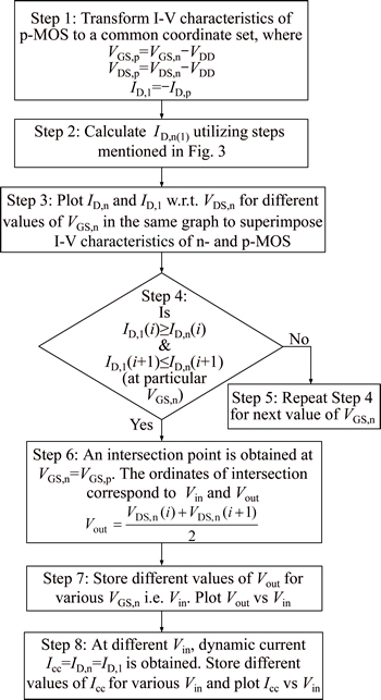
Fig. 6 Flow depicting a step-wise algorithm for obtaining voltage transfer characteristics (VTC) curve and dynamic current of s-Si/s-Si1-yGey/r-Si1-xGex MOSFET-based CMOS inverter
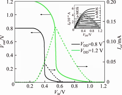
Fig. 7 Plot of VTC curve and dynamic current of s-Si/s-Si1-yGey/r-Si1-xGex MOSFET-based CMOS inverter for two different supply voltages (VDD) (Parameters corresponding to inverter-I appearing in Table 1 have been utilized. Superimposed I-V characteristics of s-Si/s-Si1-yGey/r-Si1-xGex n- and p-MOS is shown in the inset)
3.3 Noise margin
The VTC curve can also be used to obtain the noise margin of digital circuits. Noise margin, obtained from the VTC curve gives a measure of the sensitivity of the inverter to noise. To evaluate the NMs it is essential to determine VIL and VIH, which can be done by using the following transformations of drain and gate voltages into input and output voltages of the inverter. VGS,n=Vin, VDS,n=Vout, VGS,p=Vin �CVDD and VDS,p=Vout�CVDD. These are then substituted in the drain current expression, which now becomes a function of Vin and Vout. Introducing series resistance demands an iterative approach for evaluating VIL and VIH. We first show the procedure for evaluating VIH.
Step 1: Equate
 (19)
(19)
Step 2: Differentiate both sides of current expressions of Step 1 w.r.t. Vin to obtain

 (20)
(20)
Substitute dVout/dVin= -1 and compute L.H.S. and R.H.S. individually. Let M=dID,n,lin/dVin and N=dID,p,sat/ dVin.
Step 3: With the initial guess of Vin=VDD+Vth,p, Vout=0 and RSD,n=0, calculate M (initial guess for Step 6).
Step 4: With Vin=VDD+Vth,p, Vout=0 and for a known RSD,n calculate ID,n,lin through iterative technique described in Fig. 3.
Step 5: Substitute ID,n,linRSD,n along with the same assumption of Vin, Vout in Step 4 in the expression of M in Step 2 to obtain
 (21)
(21)
Step 6: Substitute M obtained in Step 3 in R.H.S. of the equation of Step 5 to obtain a new value of M.
Step 7: Substitute the newly obtained value of M from Step 6 in R.H.S. of Eq. (21). Repeat this step until M saturates.
Step 8: Repeat Steps 3 to 7 to calculate N in a similar manner.
Step 9: Substitute M and N obtained in Steps 7 and 8 respectively in Eq. (20) to obtain an equation which is a function of Vin and Vout.
Step 10: Substitute ID,n(p),lin(sat) obtained in Step 4 and a known RSD,n(p) in Eq. (19) to obtain an expression of Vout in terms of Vin.
Step 11: Substitute the above expression of Vout in the equation obtained in Step 9. Then compute Vin.
Step 12: Substitute Vin obtained from Step 11 in the expression of Vout obtained in Step 10, to compute Vout.
Step 13: Substitute the new values of Vin and Vout in Steps 3 and 4 and repeat Steps 3 to 12 until Vin and Vout saturate. The saturated value of Vin gives VIH.
Equating ID,n,sat and ID,p,lin and following the above algorithm, using Vin=Vth,n and Vout=VDD in Steps 3 and 4, VIL can also be obtained. In an effort to demonstrate the universality of our proposed algorithms, we have applied the same to evaluate the NMs of strained-Si/relaxed- Si1-xGex MOSFET-based CMOS inverter for various supply voltages with the parameters mentioned in Ref. [37] and compared with the data obtained through mixed mode analysis combining both device and circuit simulator (MEDICI and PSPICE) [37], as illustrated in Fig. 8. The series resistance required for computations was extracted from the ratio of two linear I-V characteristics [37] and following the procedure described in Ref. [21]. Our computations are in good agreement with the reported data. Average deviations of 1.0% and 3.15% were found for NML and NMH respectively, highlighting the accuracy of our proposed technique.
The plot of VIL and VIH of s-Si/s-Si1-yGey/r-Si1-xGex MOSFET-based CMOS inverter for different Ge concentrations of strained (y) and relaxed (x) layer is shown in Fig. 9(a) which has been computed with the parameters of inverter-I in Table 1. From the figure, we observe that VIL and VIH decrease with increase in strain. The result obtained is consistent with that reported in Ref. [38]. It can also be inferred from the figure that VIL and VIH increase with increase in VDD. It would be important to note here that the iteration involved in obtaining VIL and VIH may or may not converge at a single point. This is due to the iterative process and differentiation involved in Step 2 of the process flow for calculating low and high NM. The former tries to converge the input voltages while the later tries to diverge them. This leads to an oscillation around the local minima as depicted in Fig. 9(b), where VIH has been plotted with the number of iterations for two different supply voltages, VDD=0.8 V and 1.8 V. With increase in the number of iterations, the peak-to-peak value saturates and the average of the peak-to-peak value may be assumed to be the convergence point.

Fig. 8 Plot of computed NML (a) and NMH (b) of s-Si/relaxed-Si1-xGex MOSFET-based CMOS inverter for different supply voltages and validation with reported results (solid rectangle) (Parameters: Ln(p)=130 nm, Wn(p)=1 ��m, tox,n(p)=3 nm. Other parameters used in our computation appear in Ref. [37])
From the VTC curve, the inverter logic threshold voltage can also be obtained, which is an important parameter that characterizes the DC performance of CMOS inverter circuits [39]. Figure 10 shows the flow chart for calculating Vinv.
4 Results and discussion
The variation of the VTC curve of s-Si/s-Si1-yGey/ r-Si1-xGex MOSFET-based CMOS inverter for different strain configurations is shown in Fig. 11. Parameters of inverter-I shown in Table 1 have been incorporated in this computation. We observe that with increase in Ge mole fraction of strained and relaxed SiGe layer, NML decreases while NMH shows the reverse nature. This may be attributed to the transconductance ratio, ��r[f(IDRSD)]= ��n[f(IDRSD)]/��p[f(IDRSD)], which changes with strain. The change in NML and NMH with respect to unstrained (x=0, y=0) MOSFET was calculated to be 15.6% and 6.56% respectively, corresponding to x=0.3 and y=0.6. The inset shows the variation of Vinv and peak current with VDD for different strain configurations. Vinv decreases with strain while there is an increase in Icc. The variation in the VTC curve and dynamic current of s-Si/s-Si1-yGey/r-Si1-xGex MOSFET-based CMOS inverter, incorporating RSD, is shown in Fig. 12. We observe that on introducing RSD, NMH decreases while the change in NML is not significant. Such changes may be attributed to the change in transconductance ratio with S/D series resistance. From the figure, it can also be seen that the dynamic current decreases with increase in RSD. The decrease in peak current corresponding to RSD=400 �� is calculated to be 29.76 %, with respect to RSD=0 ��. The change in Vinv with VDD for different series resistances is shown in the inset of the same figure. We observe that Vinv increases with increase in RSD. Figure 13(a) shows the plot of VTC curve of s-Si/s-Si1-yGey/r-Si1-xGex MOSFET-based CMOS inverter for different widths of n-MOS. It can be observed from the figure that with increase in n-MOS width, the inverter logic threshold voltage shifts to a lower value. NML decreases while NMH shows the reverse nature with Wn, the plot of which is shown in Fig. 13(b). This is due to the change in the transconductance ratio corresponding to VIL and VIH, the plot of which is shown in Fig. 13(c), which increases with increase in Wn. This gives us an ample scope of tuning the characteristics of an inverter by introducing strain and/or by varying the device parameters. Next we focus on the impact of strain on the propagation delay of s-Si/s-Si1-yGey/r-Si1-xGex MOSFET-based CMOS inverters. PD is also one of the important performance parameters of CMOS circuits, which has received considerable attention through decades. The delay associated with charging/discharging of the output capacitor (load) heavily depends on the drive current of the device. In this work we have adopted the ��ON-resistance�� method for evaluating the PD of circuits. For this we have used a simulator which was earlier developed by our group [40]. By using the drain current equations of the strained device, as illustrated in Section 2.2, in the simulator [40], we were able to plot the PD versus gate oxide thickness for different strain configurations, as shown in Fig. 14. The value of load capacitance used in the computation has been taken from Ref. [41]. We observe that the PD increases monotonically with oxide thickness. Furthermore, the delay decreases on introducing strain. The reason may be stated as follows. Incorporating strain increases the drive current of the device. This causes an increase in the charging and discharging of the load capacitance, which ultimately increases the speed of the device. We also infer from Fig. 14 that the spread in the PD for lower gate oxide thickness is small as compared to some higher values of oxide thickness. The gate leakage current is subject to increase as the gate dielectric reduces below 2 nm due to tunneling. This in turn increases the static power consumption of the overall circuit. High-k dielectric materials [42-44] combined with SiO2 have been a traditional material manifestation to improve the performance of the device. Such gate material modification along with strained channel can further boost the performance of circuits. Figure 15 shows the variation of VTC curves with various high-k dielectrics along with metal gate. The inset shows the increase in the drain current as compared to poly-Si/SiO2. A three-fold increase in the drain current also enhances the speed of the device which is depicted in the comparative chart shown in Fig. 16.

Fig. 9 Plot of VIL and VIH of s-Si/s-Si1-yGey/r-Si1-xGex MOSFET-based CMOS inverter with VDD for various strain configurations (a) and plot showing oscillation of VIH with number of iterations for two different supply voltages (b)

Fig. 10 Flow chart depicting a step-wise algorithm for calculating inverter logic threshold voltage (Vinv) of s-Si/s-Si1-yGey/ r-Si1-xGex MOSFET-based CMOS inverter

Fig. 11 Variation of VTC curve of s-Si/s-Si1-yGey/r-Si1-xGex MOSFET-based CMOS inverter for various strain configurations (The inset shows the plot of Vinv and Icc with VDD for different mole fractions of strained (y) and relaxed (x) layer)
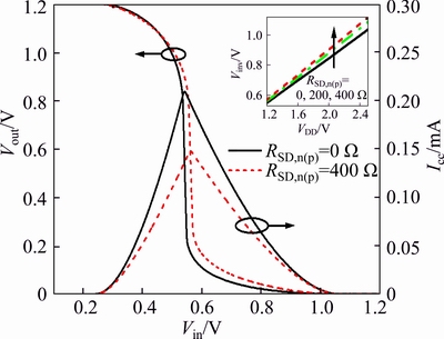
Fig. 12 Variation of computed VTC curve and dynamic current of s-Si/s-Si1-yGey/r-Si1-xGex MOSFET-based CMOS inverter for two different S/D series resistances, RSD=0 �� and 400 �� (Parameters corresponding to inverter-I in Table 1 have been utilized. The inset shows the variation of Vinv with respect to VDD for different S/D series resistances)

Fig. 13 Plot of computed VTC curve of s-Si/s-Si1-yGey/ r-Si1-xGex MOSFET-based CMOS inverter for different n-channel widths (Parameters corresponding to inverter-I in Table 1 have been utilized) (a), variation of NML and NMH with VDD for different width of n-MOS (b), plot of transconductance ratio with n-channel width for VIL and VIH (c)

Fig. 14 Variation of PD with gate oxide thickness for different strain configurations (The load capacitance has been assumed to be 32 fF [41])

Fig. 15 VTC curves for different high-k dielectric materials and metal gate (Inset shows the plot of drain current with different high-k dielectrics)

Fig. 16 Comparative plots of noise margin (NML (a) and NMH (b)) and PD (c) for various high-k dielectric materials and conventional poly-Si based circuit (Parameters corresponding to inverter-I in Table 1 have been utilized)
5 Conclusions
To summarize, we have presented a computational technique for investigating the performance parameters of s-Si/s-Si1-yGey/r-Si1-xGex MOSFETs and circuits, incorporating S/D series resistance. Flows describing step-wise algorithms have been presented which may be useful to the scientific community. The proposed algorithms are not only restricted to strained MOSFETs but can be applied to any device architectures which can be modeled by analytical expressions. Through our computations we have quantitatively established that the S/D series resistance may be responsible for a significant reduction in the drain current. We have also shown that VTC, NM, inverter logic threshold voltage and dynamic current can be tuned by incorporating various strain configurations. One of the important findings of our work is that the dynamic current flowing through an inverter, during switching activity, decreases if S/D series resistance is taken into account. The series resistance, whose contribution cannot be neglected in scaled down fabricated devices, may be considered to be a boon for CMOS inverters as it reduces the dynamic power dissipation significantly. We have also found that incorporating strain enhances the speed of inverters while the NM (particularly NML) decreases. The choice of strain configuration in s-Si/s-Si1-yGey/r-Si1-xGex MOSFETs for optimum circuit performance may be a compromise between speed and noise immunity. Although the proposed algorithm is computationally more efficient, the dependence on the analytical expressions may limit its application. However, the growing demand of analytical models may prove the proposed algorithm useful to the scientific research community. The scope of tuning the NM and switching characteristics by using high-k dielectric materials has also been presented.
References
[1] DALAPATI G K, CHATTOPADHYAY S, DRISCOLL L S, O��NEILL A G, KWA K S K, OLSEN S H. Extraction of strained-Si metal-oxide-semiconductor field-effect transistor parameters using small signal channel conductance method [J]. Journal of Applied Physics, 2006, 99(3): 034501-034508.
[2] LEE M L, FITZGERALD E A, BULSARA M T, CURRIE M T, LOCHTEFELD A. Strained Si, SiGe, and Ge channels for high-mobility metal-oxide-semiconductor field-effect transistors [J]. Journal of Applied Physics, 2005, 97(1): 011101-011127.
[3] RIM K, HOYT J L, GIBBONS J F. Fabrication and analysis of deep submicron strained-Si N-MOSFET��s [J]. IEEE Transactions on Electron Devices, 2000, 47(7): 1406-1415.
[4] FOSSUM J G, ZHANG W. Performance projections of scaled CMOS devices and circuits with strained Si-on-SiGe channels [J]. IEEE Transactions on Electron Devices, 2003, 50(4): 1042-1049.
[5] WANG Bin, ZHANG He-ming, HU Hui-yong, ZHANG Yu-ming, ZHOU Chun-yu, LI Yu-chen. Effect of substrate doping on threshold voltages of buried channel pMOSFET based on strained-SiGe technology [J]. Journal of Central South University, 2014, 21: 2292-2297.
[6] FLACHOWSKY S, WEI A, ILLGEN R, HERRMANN T, HONTSCHEL J, HORSTMANN M, KLIX W, STENZEL R. Understanding strain-induced drive-current enhancement in strained-silicon n-MOSFET and p-MOSFET [J]. IEEE Transactions on Electron Devices, 2010, 57(6): 1343-1354.
[7] AUTH C, CAPPELLANI A, CHUN J S, DALIS A, DAVIS A, GHANI T, GLASS G, GLASSMAN T, HARPER M, HATTENDORF M, HENTGES P, JALOVIAR S, JOSHI S, KLAUS J, KUHN K, LAVRIC D, LU M, MARIAPPAN H, MISTRY K, NORRIS B, RAHHAL-ORABI N, RANADE P, SANDFORD J, SHIFREN L, SOUW V, TONE K, TAMBWE F, THOMPSON A, TOWNER D, TROEGER T, VANDERVOORN P, WALLACE C, WIEDEMER J, WIEGAND C. 45 nm high-k + metal gate strain-enhanced transistors [C]// Symposium on VLSI Technology Digest of Technical Papers. Honolulu, HI, USA: IEEE, 2008: 128-129.
[8] CHEN C H, LEE T L, HOU T H, CHEN C L, CHEN C C, HSU J W, CHENG K L, CHIU Y H, TAO H J, JIN Y, DIAZ C H, CHEN S C, LIANG M S. Stress memorization technique (SMT) by selectively strained-nitride capping for sub-65nm high-performance strained-Si device application [C]// Symposium on VLSI Technology Digest of Technical Papers. Honolulu, HI, USA: IEEE, 2004: 56-57.
[9] GHANI T, ARMSTRONG M, AUTH C, BOST M, CHARVAT P, GLASS G, HOFFMANN T, JOHNSON K, KENYON C, KLAUS J, MCINTYRE B, MISTRY K, MURTHY A, SANDFORD J, SILBERSTEIN M, SIVAKUMAR S, SMITH P, ZAWADZKI K, THOMPSON S, BOHR M. A 90 nm high volume manufacturing logic technology featuring novel 45 nm gate length strained silicon CMOS transistors [C]// IEEE IEDM Technical Digest. Washington DC, USA: IEEE, 2003: 978-980.
[10] ANG K W, CHUI K J, BLIZNETSOV V, DU A, BALASUBRAMANIAN N, LI M F, SAMUDRA G, YEO Y C. Enhanced performance in 50 nm n-MOSFETs with silicon-carbon source/drain regions [C]// IEEE IEDM Technical Digest. San Francisco, CA, USA: IEEE, 2004: 1069-1071.
[11] CURRIE M T, LEITZ C W, LANGDO T A, TARASCHI G, FITZGERALD E A, ANTONIADIS D A. Carrier mobilities and process stability of strained Si n- and p-MOSFETs on SiGe virtual substrates [J]. Journal of Vacuum Science & Technology B, 2001, 19(6): 2268-2279.
[12] LEITZ C W, CURRIE M T, LEE M L, CHENG Z Y, ANTONIADIS D A, FITZGERALD E A. Hole mobility enhancements in strained Si/Si1-yGey p-type metal-oxide-semiconductor field-effect transistors grown on relaxed Si1-xGex (x [13] CHENG Z, JUNG J, LEE M L, PITERA A J, HOYT J L, ANTONIADIS D A, FITZGERALD E A. Hole mobility enhancement in strained-Si/strained-SiGe heterostructure p-MOSFETs fabricated on SiGe-on-insulator (SGOI) [J]. Semiconductor Science and Technology, 2004, 19: L48-L51. [14] JUNG J, YU S, LEE M L, HOYT J L, FITZGERALD E A, ANTONIADIS D A. Mobility enhancement in dual-channel P-MOSFETs [J]. IEEE Transactions on Electron Devices, 2004, 51(9): 1424-1431. [15] LEE M L, FITZGERALD E A. Hole mobility enhancements in nanometer-scale strained-silicon heterostructures grown on Ge-rich relaxed Si1-xGex [J]. Journal of Applied Physics, 2003, 94(4): 2590-2596. [16] TSANG Y L, CHATTOPADHYAY S, UPPAL S, ESCOBEDO- COUSIN E, RAMAKRISHNAN H K, OLSEN S H, O��NEILL A G. Modeling of the threshold voltage in strained Si/Si1-xGex/Si1-yGey (x �� y) CMOS architectures [J]. IEEE Transactions on Electron Devices, 2007, 54(11): 3040-3048. [17] JUNG J, YU S, OLUBUYIDE O O, HOYT J L, ANTONIADIS D A, LEE M L, FITZGERALD E A. Effect of thermal processing on mobility in strained Si/strained Si1-yGey on relaxed Si1-xGex (x [18] OLSEN S H, O��NEILL A G, CHATTOPADHYAY S, DRISCOLL L S, KWA K S K, NORRIS D J, CULLIS A G, PAUL D J. Study of single- and dual-channel designs for high-performance strained-Si-SiGe n-MOSFETs [J]. IEEE Transactions on Electron Devices, 2004, 51(7): 1245-1253. [19] CHUN S K, WANG K L. Effective mass and mobility of holes in strained Si1-xGex layers on (001) Si1-yGey substrate [J]. IEEE Transactions on Electron Devices, 1992, 39(9): 2153-2164. [20] LIN Da-wen, CHENG Ming-lung, WANG Shyh-wei, WU Chung-Cheng, CHEN Ming-Jer. A novel method of MOSFET series resistance extraction featuring constant mobility criteria and mobility universality [J]. IEEE Transactions on Electron Devices, 2010, 57(4): 890-897. [21] CAMPBELL J P, CHEUNG K P, SUEHLE J S, OATES A. A simple series resistance extraction methodology for advanced CMOS devices [J]. IEEE Electron Device Letters, 2011, 32(8): 1047-1049. [22] BINDU B, DASGUPTA N, DASGUPTA A. Analytical model of drain current of strained-Si/strained-Si1-YGeY/relaxed-Si1-XGeX NMOSFETs and PMOSFETs for circuit simulation [J]. Solid-State Electronics, 2006, 50(3): 448-455. [23] ENGSIEW K, ANWAR S, ISMAIL R. Quantum mechanical effects on the threshold voltage of nanoscale dual channel strained Si/strained Si1-yGey/relaxed Si1-xGex MOSFETs [J]. Journal of Computational and Theoretical Nanoscience, 2013, 10(5): 1231-1235. [24] RABAEY J M, CHANDRAKASAN A, NIKOLIC B. Digital integrated circuits: A design perspective [M]. New Jersey: Pearson Education, 2003. [25] PSPICE User��s manual [M]// Cadence ORCAD 16.6. San Jose, CA, USA: Cadence Design Systems Inc, 2012. [26] TANNER Tools user��s manual [M]. Monrovia, CA: Tanner Research Inc, 2006. [27] ATLAS Users manual [M]. Santa Clara, CA, USA: Silvaco Inc, 2012. [28] TAURUS MEDICI user guide [M]. Mountain View, CA, USA: Synopsys Inc, 2012. [29] TABERKIT A M, BOUAZZA-GUEN A. Engineering of nano-scale strained-MOSFETs: A solution for the mobility enhancement [J]. World Academy of Science, Engineering and Technology, International Journal of Electrical, Computer, Energetic, Electronic and Communication Engineering, 2015, 9(12): 1330-1333. [30] TANG Zhao-huan, TAN Kai-zhou, CUI Wei, WANG Bin. ��MAX enhanced 190% of a strained NMOS based on SiGe virtual substrate [J]. Advanced Materials Research, 2013, 756�C759: 154-157. [31] YU J, WANG C, YANG Y. Progress on the numerical calculation of electrical characteristics of strained SiGe channel p-MOSFET [J]. Applied Mechanics and Materials, 2013, 320: 465-472. [32] ARORA N. MOSFET modeling for VLSI simulation: Theory and practice [M]. Singapore: World Scientific, 2007. [33] RIM K, CHU J, CHEN H, JENKINS K A, KANARSKY T, LEE K, MOCUTA A, ZHU H, ROY R, NEWBURY J, OTT J, PETRARCA K, MOONEY P, LACEY D, KOESTER S, CHAN K, BOYD D, IEONG M, WONG H S. Characteristics and device design of sub-100 nm strained Si n- and p-MOSFETs [C]// Symposium on VLSI Technology Digest of Technical Papers. Honolulu, HI, USA: IEEE, 2002: 98-99. [34] JUNG J, LEE M L, YU S, FITZGERALD E A, ANTONIADIS D A. Implementation of both high-hole and electron mobility in strained Si/strained Si1-yGey on relaxed Si1-xGex [35] TEMPLE M P, PAUL D J, TANG Y T, WAITE A M, EVANS A G R, O��NEILL A G, ZHANG J, GRASBY T, PARKER E H C. The relative performance enhancement of strained-Si and buried channel p-MOS as a function of lithographic and effective gate lengths [C]// International Semiconductor Device Research Symposium. Washington DC, USA: IEEE, 2003: 51-52. [36] BSIM Model. [2013-11-01]. http://www-device.eecs.berkeley. edu/bsim. [37] RAMAKRISHNAN H. Strained silicon technology for low-power high-speed circuit applications [R]. U.K.: Newcastle University, 2008. [38] HWANG J R, HO J H, TING S M, CHEN T P, HSIEH Y S, HUANG C C, CHIANG Y Y, LEE H K, LIU A, SHEN T M, BRAITHWAITE G, CURRIE M, GERRISH N, HAMMOND R, LOCHTEFELD A, SINGAPOREWALA F, BULSARA M, XIANG Q, LIN M R, SHIAU W T, LOH Y T, CHEN J K, CHIEN S C, WEN F. Performance of 70 nm strained-silicon CMOS devices [C]// Symposium on VLSI Technology Digest of Technical Papers. Kyoto, Japan: IEEE, 2003: 103-104. [39] KANG S M, LEBLEBICI Y. CMOS digital integrated circuits: analysis and design [M]. New York: McGraw�CHill, 2003. [40] KUMAR S, JHA S. Impact of elliptical cross-section on the propagation delay of multi-channel gate-all-around MOSFET based inverters [J]. Microelectronics Journal, 2013, 44: 844-851. [41] FITZGERALD E A, GERRISH N. CMOS inverter and integrated circuits utilizing strained silicon surface channel MOSFETS: US, 0034529 [P]. 2003. [42] FRANCO J, KACZER B, MITARD J, TOLEDANO-LUQUE M, ROUSSEL P J, WITTERS L, GRASSER T, GROESENEKEN G. NBTI reliability of SiGe and Ge channel pMOSFETs with SiO2/HfO2 dielectric stack [J]. IEEE Transactions on Device and Materials Reliability, 2013, 13(4): 497-506. [43] BEISTER J, WACHOWIAK A, BOSCHKE R, HERRMANN T, UHLARZ M, MIKOLAJICK T. Mobility investigations on strained 30-nm high-k metal gate MOSFETs by geometrical magnetoresistance effect [J]. IEEE Transactions on Electron Devices, 2015, 62(6): 1819-1825. [44] GHOSH K, DAS S, FISSEL A, OSTEN H J, LAHA A. Epitaxial Gd2O3 on strained Si1-xGex layers for next generation complementary metal oxide semiconductor device application [J]. Applied Physics Letters, 2013, 103(15): 153501-153504. (Edited by YANG Hua) Cite this article as: Kumar Subindu, Kumari Amrita, Das Mukul K. Strain induced changes in performance of strained-Si/strained-Si1-yGey/relaxed-Si1-xGex MOSFETs and circuits for digital applications [J]. Journal of Central South University, 2017, 24(6): 1233-1244. DOI: 10.1007/s11771-017-3527-4. Received date: 2016-02-26; Accepted date: 2016-09-30 Corresponding author: Kumar Subindu, Assistant Professor; Tel: +91-326-2235732; E-mail: subindu.kumar.1976@ieee.org virtual [J]. Letters, p substrate IEEE Electron Device 2003, 24(7): 460-462.

