Effect of surface nanocrystallization and PPEC time oncomplex nanocrystalline hard layer fabricated by plasma electrolysis
来源期刊:中国有色金属学报(英文版)2010年第3期
论文作者:M. ALIOFKHAZRAEI SH. AHANGARANI A. Sabour Rouhaghdam
文章页码:425 - 431
Key words:surface nanocrystallization; hard layer; roughness; CP-Ti
Abstract: Size distribution of nano-carbides produced by duplex treatments of surface nanocrystallization (by surface severe plastic deformation) and plasma electrolytic carburizing on CP-Ti was investigated. Skewness and kurtosis of Gussian shape distribution curves were studied and the effect of time was determined. The usage of longer time is more suitable for achieving less size of complex nano-carbides. Surface roughness of treated samples was measured. It is observed that there is an optimum level for time on surface roughness increasing (difference between two measured data).

M. ALIOFKHAZRAEI1, SH. AHANGARANI2, A. SABOUR ROUHAGHDAM1
1. Department of Materials Engineering, Faculty of Engineering, Tarbiat Modares University,P.O. Box: 14115-143, Tehran, Iran;
2. Department of Advanced Materials and Renewable Energies,
Iranian Research Organization for Science and Technology (IROST), P.O. Box 15815-3538, Tehran, Iran
Received 22 January 2009; accepted 2 April 2009
Abstract: Size distribution of nano-carbides produced by duplex treatments of surface nanocrystallization (by surface severe plastic deformation) and plasma electrolytic carburizing on CP-Ti was investigated. Skewness and kurtosis of Gussian shape distribution curves were studied and the effect of time was determined. The usage of longer time is more suitable for achieving less size of complex nano-carbides. Surface roughness of treated samples was measured. It is observed that there is an optimum level for time on surface roughness increasing (difference between two measured data).
Key words: surface nanocrystallization; hard layer; roughness; CP-Ti
1 Introduction
Diffusion processes can exert significant influence on the different properties of many alloys. Among them, titanium based alloys are used for fabrication of components of aerospace engines. The innovation of appropriate new coatings with improved performance for titanium is still an interesting and important research area. One way to improve the surface hardness and passive layer stability of different kinds of titanium based alloys is using plasma electrolysis technique[1]. Pulsed plasma electrolytic carburizing (PPEC) technique is a relatively new group of saturation treatments which has been used to different metals[2]. Electrolytes of this electrolytic method are ecologically friendly and non-hazardous[3].
Despite the considerable effort that has been invested into understanding the different properties of treated steels, it seems that little attention has been given to the role of PPEC in wear and corrosion procedure. Deep understanding of the subject cannot be achieved without a clear view of the role of morphology of the nanostructured layers. It is, therefore, the aim of this work to further clarify the important role of nanocrystalline carburized layer and its characteristics and changes with respect to the effective factors of coating process.
Nanocrystalline carburized layers can be synthesized successfully through pulsed plasma electrolytic carburizing method, which is caused by the bombardment of the sample in an organic based electrolyte[4]. It is obviously found that there is a direct relationship between the nanostructure of compound layer and its properties. Considering Gussian shape of normal distribution for achieved nano-carbides, it is better to have a normal distribution with its specific kurtosis and skewness levels. So, in this work, the surface roughness of pulsed plasma electrolytic carburized CP-Ti was studied with respect to different deviations from normal status. Up to fourth moment, distribution of nano-carbides has been studied and they revealed direct relation with roughnesses of differently treated samples.
2 Experimental
2.1 Materials and treatments
A set of samples was machined from a d20 mm rod of CP-Ti. The sample is a cylinder of 5 mm in length and 20 mm in diameter with a small hole (d4 mm) at its surrounding area for holding. Specimens were ground with SiC emery paper up to 2 500 grit, cleaned with distilled water and degreased with acetone in an ultrasonic bath for 10 min before the treatment.
2.2 Duplex treatments
For surface nanocrystallization (SN) process, samples were subjected in the cylindrical steel container of a high energy mill with enough WC/Co balls (d6 mm) for 3 h under vacuum condition[5-6]. The average size of nanocrystals for all samples was obtained to be about 68 nm after this treatment. After surface nano- crystallization, PPEC treatment was conducted by a 30 kW power supply for obtaining nanocrystalline hard carbide based layer on pre-nanocrystalline surface of CP-Ti samples. It was performed with an electrical DC source and a pulser box. A cooling system was used for controlling the electrolyte temperature. The experimental set-up can be found in our previous articles[7]. After loading the sample, the carburizing reactor was circulated for purpose of cooling by a pump and the sample was located in the middle of cylinder shape stainless steel anode. The sample was then treated at 0.5 A/cm2 of average current density, 5 kHz of frequency and 40% of duty cycle for monopolar pulsed current for different treatment times. The resulting sparks then bombards the sample with high-energy radicals and produces carburized surface. The distance between the cathode and anode was 50 mm. The samples were allowed to cool down to room temperature from the carburizing temperature by taking them out during sparking from the reactor.
2.3 Analysis
Surface roughness of treated samples was measured via a Taylor-Hobson Surtronic 25 roughness checker. The obtained data were analyzed by Talyprofile (Gold) software. To measure average size of nanocrystallites, five SEM nanostructures from each sample with the same magnification were analyzed through commercial software for figure analysis called a4iDocu for each treated sample. Scanning electron microscopy (SEM) was performed using a Philips XL-30. Nanostructures of layers have been analyzed by transmission electron microscope (TEM, CM200-FEG-Phillips). Different measurements were interpolated to obtain average results. At least 40 measurements were done in each nanostructure for minimizing systematical errors. The size distribution of nanocrystals was plotted and it has shown a Gaussian-shape. Different treatment times of PPEC sample will cause different distributions of nanocrystalline carbides, so several different distributions (for several treatment times) have been used to give a more accurate fit to the average size of nanocrystallites than that using a Gaussian distribution. The nanostructure of coating was evaluated also by atomic force microscopy (AFM). The AFM part was a NanoScope Ⅱ from Digital Instruments, USA. Non-scraping Si3N4-tips were used throughout. In order to obtain realistic profiles, the first four moments of the distribution functions must be taken into account:
![]() (1)
(1)
![]() (2)
(2)
![]() (3)
(3)
![]() (4)
(4)
The first moment Rp, known as the range, refers to the peak of the distribution. The range is the average size of nanocrystallites at the maximum value of distribution and does not affect the shape of the profile. The second moment ΔR or straggle, gives the width of the distribution. The normalized third moment γ indicates the skewness for a given distribution profile:
![]() (5)
(5)
It will have a value of zero for a pure Gaussian distribution. If the skewness is negative, the distribution falls toward the surface more smoothly and decreases sharply on the other side of the distribution peak. The steepness of the slopes is opposite for positive skewness. The normalized fourth moment β, called kurtosis, describes the extent of the tail for any distribution:
![]() (6)
(6)
Kurtosis also indicates whether a distribution is sharply peaked or more flat topped. A distribution with a high value for kurtosis will be sharply peaked with a long exponential tail. For a pure Gaussian distribution, the kurtosis has a value of 3. Schematic maps of kurtosis and skewness and their changes can be seen in Fig.1.
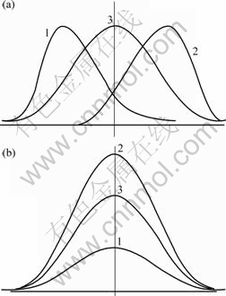
Fig.1 Schematic changes of kurtosis and skewness of distribution curves: (a) 1―Positive skewness, 2―Negative skewness, 3―Skewness=0, for normal distribution; (b) 1―Kurtosis<3, 2―Kurtosis>3, 3―Kurtosis=3, for normal distribution
3 Results
For each reported data, three events were calculated to achieve sufficient accuracy. Fig.2 is an example of achieved nanocrystallites during the carburizing process. Four parameters that are extracted from the best fit of the distribution functions are shown in Figs.3(a)-(d). For the range in Fig.3(a), linear relationship is obtained with treatment time. The results for the straggle show the same curvature as a function of treatment time in Fig.3(b).

Fig.2 Nano-carbides fabricated at different treatment time ((a) 17 min; (b) 24 min) and their AFM nanostructure (c)

Fig.3 Different obtained parameters from distribution curves versus time for PPEC treatment: (a) Range; (b) Straggle; (c) Skewness; (d) Kurtosis
4 Discussion
4.1 Plasma electrolytic carburizing
4.1.1 Effect of treatment time on size distribution of nanocrystallites
Changes of different moments of distribution have been shown in Figs.3(a)-(d) during surface hardening. It has been revealed that different moments of distribution change linearly with increasing treatment time during coating process. Treatment time in this process is the most important factor to identify the thickness of hard layer. By increasing the treatment time, diffusive radicals will bombard surface of the sample more and more and the average size of nanocrystallites will decrease. Normal distribution of nanocrystallites will be obtained at the treatment time near 35 min and it can be seen from Figs.3(c) and 3(d) (for skewness of 0 and kurtosis of 3).
4.1.2 Effect of treatment time on roughness increasing
It is a common knowledge that the best properties of nanocrystallites can be achieved at their normal narrow size distribution, so the changes of one important related property of coatings to the distribution of nanocrystallites (surface roughness) are plotted in Fig.4. It can be seen that the roughness of the coating will increase slightly by increasing the treatment time, but the amount of roughness increasing (difference among each two measured data), will decrease toward 35 min and increase after that, which means that, from this point of view, 35 min of treatment time is an optimum level. In fact, increasing the treatment time will cause two inverse effects (decreasing the average size of nanocrystallites and increasing the harmful effect of micro and nano explosions (sparks)) on the roughness of treated sample. The optimum level is 35 min for treatment time. This optimum level is the point at which the distribution of nanocrystallites is in its normal mode. By increasing the skewness and kurtosis of distribution toward its normal mode, however, the effect of sparks on total profile of the surface is larger than the shape of nanocrystallites, but the amount of increasing roughness will decrease. Increasing skewness and kurtosis of distribution after its normal mode will increase roughness, which usually is not appropriate in industrial usages.

Fig.4 Roughness increasing versus time for PPEC treatment
4.2 Surface nanocrystallization and plasma electrolytic carburizing
4.2.1 Effect of treatment time on distribution of nanocrystallites
Figs.5(a)-(d) illustrate the changes for different moments of distribution during duplex treatment. All of the changes are similar to the PPEC treatment without surface nanocrystallization. Somehow, the average size of nanocrystallites has been changed. The regressed equations for voltage can again be expressed linearly. It appears that the effect of surface nanocrystallization and residual stresses just show itself on the growth mechanism of nanocrystallites and their average size and do not affect the relation of treatment time on duplex process. By increasing the treatment time, more diffusive radicals will bombard nanocrystalline surface and the relation between treatment time and distribution of nanocrystallites remains its linear status. Normal distribution of nanocrystallites will be obtained at the treatment time near 30 min and it can be seen from Figs.3(c) and 3(d) (for skewness of 0 and kurtosis of 3). It is also obvious that the effect of surface nanocrystallization is reducing the treatment time for achieving normal distribution.

Fig.5 Different obtained parameters from distribution curves versus time for duplex treatments: (a) Range; (b) Straggle; (c) Skewness; (d) Kurtosis
4.2.2 Effect of treatment time on roughness increasing
The changes of surface roughness of coatings are plotted in Fig.6. Roughness will increase itself due to duplex treatment, but the amount of its increasing will show a similar trend as single PPEC treatment. The amount of roughness increasing (difference between two measured data) will decrease toward 30 min and increase after that, which means that again, 30 min of treatment time is an optimum level. Increasing the effect of micro and nano sparks has larger effect on roughness than decreasing the average size of nanocrystallites, which leads to higher surface roughness for duplex treatment than single PPEC treatment but the roughness increasing is smaller in amount for duplex treatment. Also the optimum level is around 30 min for treatment time.

Fig.6 Roughness increasing versus time for duplex treatments
Fig.7 shows the TEM nanostructure of coatings which have been fabricated by PPEC (7a) and pre surface nanocrystallization with PPEC (7b). It can easily be seen that average sizes of nanocrystallites are decreased by pre surface nanocrystallization. This effect probably is due to locking of dislocation networks for deformed surfaces which can cause low average size of fabricated nanocrystallites.

Fig.7 TEM nanostructure (BFI) of fabricated layers with PPEC treatment (a) and pre surface nanocrystallization with PPEC treatment (b)
4.3 Effect of treatment time on growth kinetics for obtained layers
It has been revealed that the thickness of the diffusive layer or compound layer for cathodic plasma electrolytic saturation treatments changes linearly with the square root of the treatment time[7]. The thickness of each layer was measured on the cross section of treated samples. The thickness of layers fabricated in a constant time, increases with the increase in the time of the carburizing treatment. Also, surface nanocrystallization (SN) process causes rapid formation of layers and thus the layer thickness in equal carburizing time and treatment time is larger than that without pre SN treatment. The increase in the thicknesses of layers proceeds in accordance with the linear relation which becomes non-linear for duplex treatment. Due to different mechanisms of carburizing processes that work in accelerating the carbon radicals with those that work in thermal activation and diffusion at long times, equations about growth kinetics of this method present here by formula resulted from interpolating different obtained data for effective factors with Rfitting≥0.98. Eq.(7) shows the relationship between thickness of influenced layer (total thickness of the layer with increased hardness in raw sample and the compound layer) and treatment time:
![]() (7)
(7)
where Th and t are thickness of influenced layer and treatment time during carburizing treatment, respectively. α and β are constants related to applied voltage for α and modified transmission coefficient of treated media for β.
By applying pre SN process, above equation is modified in this way:
![]() (8)
(8)
As it can be seen from Eq.(8), Th? increases more rapidly than Th, compared with Eq.(7). In fact, SN process affects formation mechanism of nanocrystalline carbide layer more than the shape or properties of carbides nanocrystallites. Nanocrystalline surface of substrate will lead to faster formation of hard layer with less treatment time than microcrystalline surface.
5 Conclusions
1) Normal distribution of nanocrystallites will be obtained at the treatment time near 35 min.
2) Increasing the treatment time will cause two inverse effects (decreasing of average size of nanocrystallites and increasing the destructive effect of sparks) on the roughness of treated sample. The optimum treatment time is 35 min.
3) Increasing skewness and kurtosis of distribution after its normal mode will increase roughness, which is usually not appropriate in industrial usages.
4) Surface nanocrystallization will affect the growth mechanism and roughness of hard layer; while its affect on thickness growth is more than roughness.
5) Under similar conditions, nanocrystalline surface of substrate will lead to faster formation of hard layer with less treatment time than microcrystalline surface.
6) TEM nanostructures confirm decreasing of average size of nanocrystallites after duplex treatments. This phenomenon is probably due to locking of dislocation networks for deformed surfaces which can cause lower average size of fabricated nanocrystallites.
Acknowledgements
The authors wish to express their thanks to Dr. J. Curran (Cambridge University) for his useful guides during the investigation of different aspects of plasma electrolysis and also Dr. S. NADIM for TEM analysis. Partial work of this project funded by National Elite Foundation of Iran and Iranian Nanotechnology Initiative is appreciated.
References
[1] NIE X, TSOTSOS C, WILSON A, YEROKHIN A L, LEYLAND A, MATTHEWS A. Characteristics of a plasma electrolytic nitrocarburising treatment for stainless steels [J]. Surface and Coatings Technology, 2001, 139: 135-142.
[2] ALIOFKHAZRAEI M, MOFIDI S H H, SABOUR ROUHAGHDAM A, MOHSENIAN E. Duplex surface treatment of pre-electroplating and pulsed nanocrystalline plasma electrolytic carbonitriding of mild steel [J]. Journal of Thermal Spray Technology, 2008, 17: 323-328.
[3] TARAKCI M, KORKMAZ K, GENCER Y, USTA M. Plasma electrolytic surface carburizing and hardening of pure iron [J]. Surface and Coatings Technology, 2005, 199(2/3): 205-212.
[4] ALIOFKHAZRAEI M, SABOUR ROUHAGHDAM A, HEYDARZADEH A. Strong relation between corrosion resistance and nanostructure of compound layer of treated 316 austenitic stainless steel [J]. Materials Characterization, 2009, 60(2): 83-89.
[5] LU K, LU J. Nanostructured surface layer on metallic materials induced by surface mechanical attrition treatment [J]. Materials Science and Engineering A, 2004, 375/377: 38-45.
[6] LU K. Nanocrystalline metals crystallized from amorphous solids: Nanocrystallization, structure, and properties [J]. Materials Science and Engineering R, 1996, 16: 161-221.
[7] ALIOFKHAZRAEI M, SABOUR ROUHAGHDAM A. A novel method for preparing aluminum diffusion coating by nanocrystalline plasma electrolysis [J]. Electrochemistry Communications, 2007, 9: 2686-2691.
Corresponding author: A. Sabour Rouhaghdam; Tel: +98-912-6905626; Fax: +98-21-66960664; E-mail: sabour01@gmail.com; sabour@modares.ac.ir
DOI: 10.1016/S1003-6326(09)60157-6
(Edited by YANG Bing)

